Method to improve ignition in plasma etching or plasma deposition steps

a technology of plasma etching and plasma deposition, which is applied in the direction of chemical vapor deposition coating, coating, electric discharge tube, etc., can solve the problem that the ignition of other materials is typically difficult in the plasma etching apparatus, and achieve the effect of increasing the ignitability of the etchant source gas

Inactive Publication Date: 2007-10-09
ADVANCED MICRO DEVICES INC
View PDF18 Cites 8 Cited by
  • Summary
  • Abstract
  • Description
  • Claims
  • Application Information

AI Technical Summary

Benefits of technology

[0009]In one embodiment, the present invention relates to a method for etching at least a portion of at least one layer of a semiconductor wafer to expose one or more underlying layers, the method comprising: placing a semiconductor wafer in a plasma reactor; supplying an etchant source gas to the plasma reactor, the etchant source gas comprising: (a) at least one reactive compound; and (b) at least one ignition gas, wherein the at least one ignition gas increases the ignitability of the etchant source gas as compared to the ignitability of the etchant source gas lacking the at least one ignition gas; igniting the etchant source gas via the application of a RF (radio frequency) energy source; and etching at least a portion of the at least one layer in the semiconductor wafer.
[0010]In another embodiment, the present invention relates to a method for increasing the ignition reliability of a plasma in a plasma reactor, the method comprising: supplying a source gas to the plasma reactor, the source gas comprising: (a) at least one reactive compound; and (b) at least one ignition gas, wherein the at least one ignition gas increases the ignitability of the source gas as compared to the ignitability of the source gas lacking the at least one ignition gas.
[0011]In another embodiment, the present invention relates to a method for plasma deposition of at least one layer over at least a portion of one or more underlying layers, the method comprising: placing a semiconductor wafer in a plasma reactor; supplying a deposition source gas to the plasma reactor, the deposition source gas comprising: (a) at least one reactive compound; and (b) at least one ignition gas, wherein the at least one ignition gas increases the ignitability of the deposition source gas as compared to the ignitability of the deposition source gas lacking the at least one ignition gas; igniting the deposition source gas via the application of a RF energy source; and depositing at least one layer over at least a portion of one or more underlying layers in the semiconductor wafer.

Problems solved by technology

As is known to those of skill in the art, the various chemistries utilized to etch such insulation layers and / or metal layers, and in the plasma deposition of other materials are typically difficult to ignite reliably in a plasma etching apparatus.

Method used


Image

  • Method to improve ignition in plasma etching or plasma deposition steps
  • Method to improve ignition in plasma etching or plasma deposition steps

Examples


Embodiment Construction

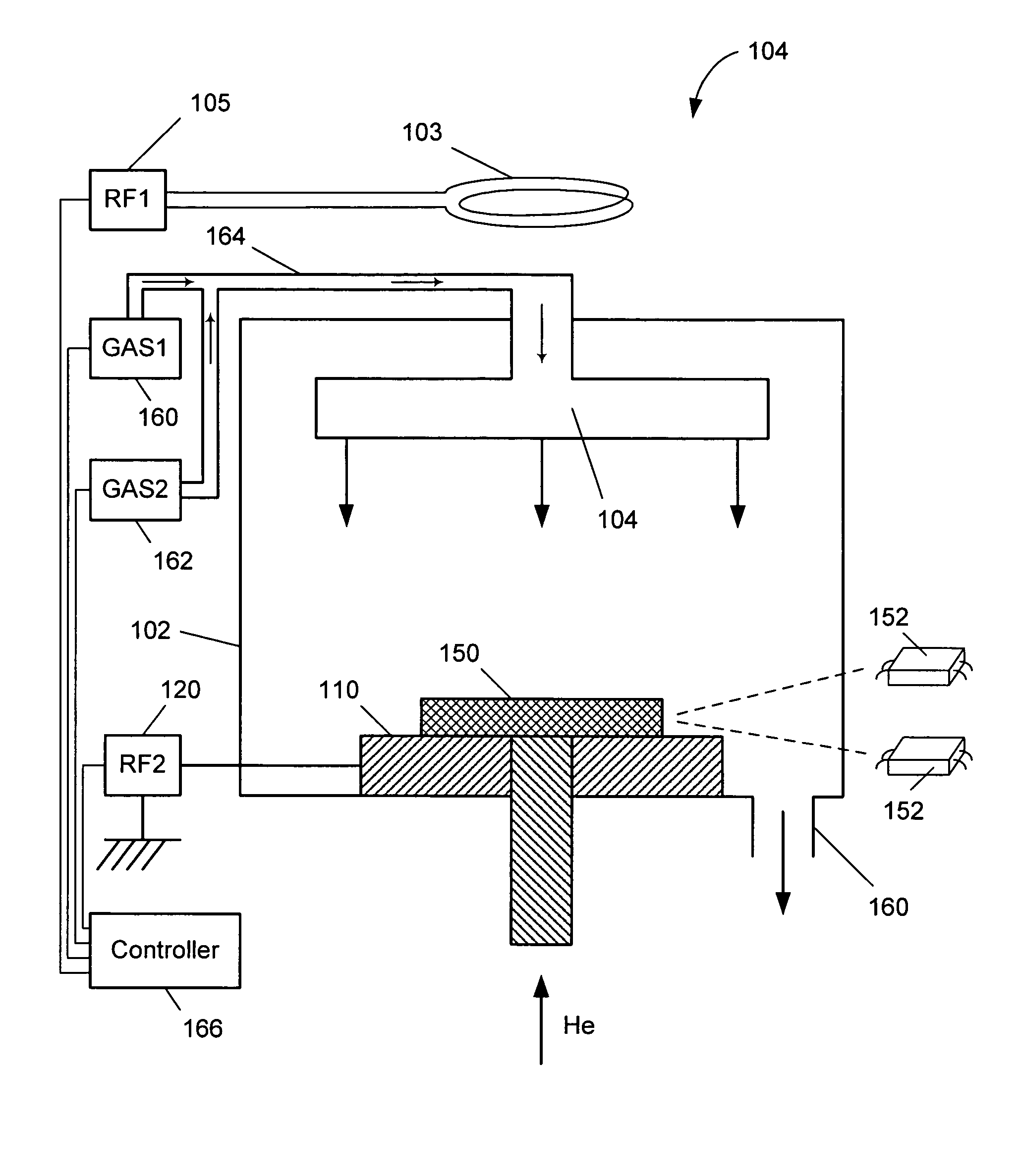
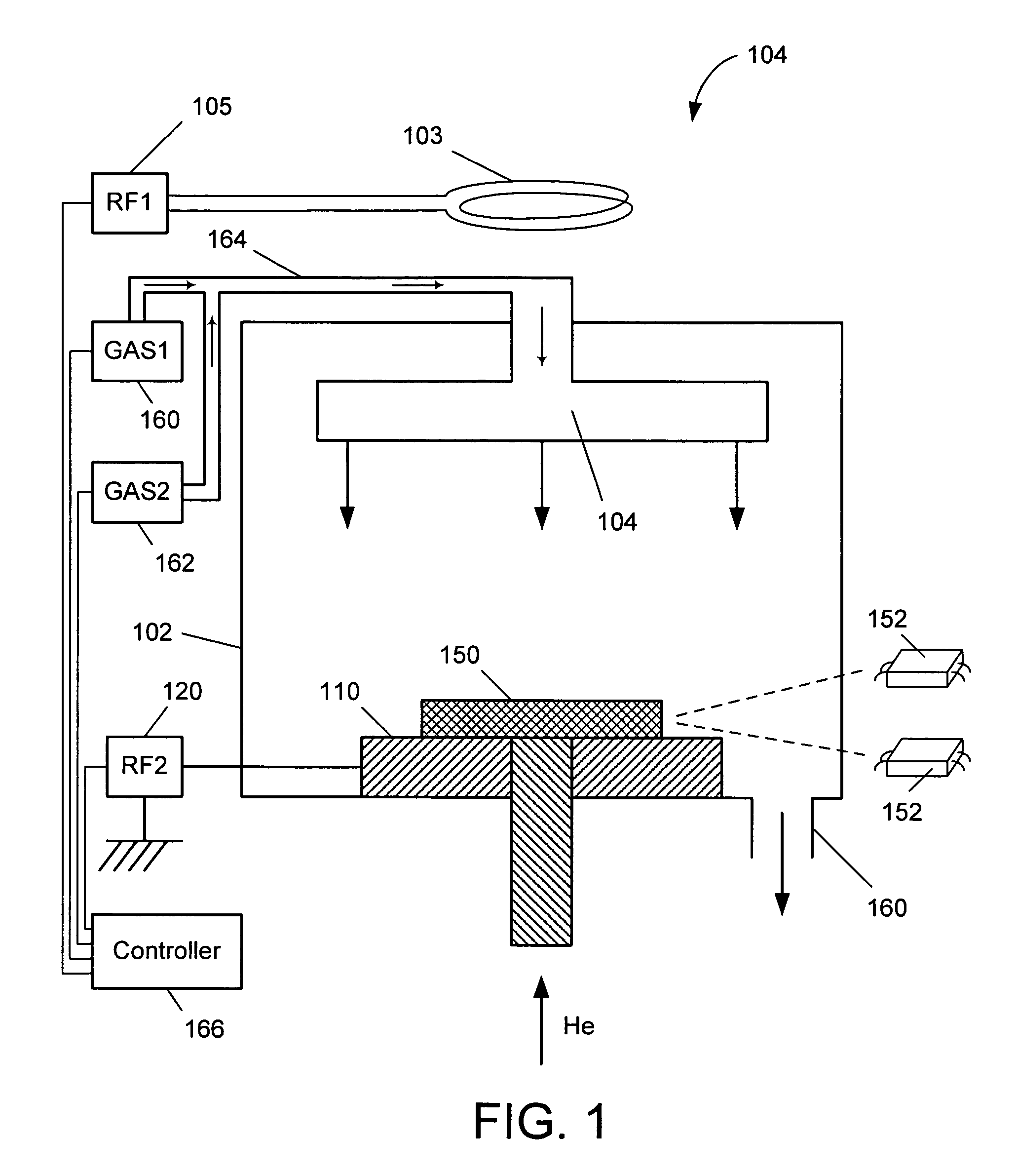
[0014]An invention is described for increasing the reliability of the ignition of an etch chemistry in a plasma reactor. The present invention also applies to increasing the reliability of the ignition of a plasma deposition chemistry in a plasma reactor.

[0015]In one embodiment of the present invention, an etchant source gas (i.e., etch chemistry or feed gas) and / or an deposition source gas (i.e., deposition chemistry) comprises at least one reactive compound (e.g., a fluorocarbon compound) and at least one ignition gas, wherein the at least one ignition gas increases the ignitability of the etchant source gas and / or deposition source gas as compared to the ignitability of an etchant source gas and / or deposition source gas lacking at least one ignition gas. Thus, in this embodiment, the etchant source gas and / or deposition source gas is at least a two-component gas. As used in the specification and claims, the term “two-component gas” encompasses both etchant source gases and deposi...


PUM

PropertyMeasurementUnit
temperatureaaaaaaaaaa
pressureaaaaaaaaaa

Abstract

In one embodiment, the present invention relates to a method for increasing the ignition reliability of a plasma in a plasma reactor, the method comprising: supplying a source gas to the plasma reactor, the source gas comprising: (a) at least one reactive compound; and (b) at least one ignition gas, wherein the at least one ignition gas increases the ignitability of the source gas as compared to the ignitability of the source gas lacking the at least one ignition gas.

Description

FIELD OF THE INVENTION[0001]The present invention relates to plasma etching or plasma deposition methods for use in semiconductor fabrication. More particularly, the present invention relates to methods by which to improve ignition reliability in plasma etching and / or plasma deposition steps in semiconductor fabrication.BACKGROUND OF THE INVENTION[0002]During the formation of semiconductor devices, such as dynamic random access memories (DRAMs), static random access memories (SRAMs), microprocessors, etc., various layers are subject to either plasma etching, plasma deposition or both.[0003]For example, insulating layers, such as silicon dioxide, phosphorous doped silicon dioxide, or other doped oxide, are used to electrically separate conductive layers, such as doped polycrystalline silicon, doped silicon, aluminum, refractory metal silicides, etc. It is often required that the conductive layers be interconnected through holes in the insulating layer. Such holes are commonly referre...

Claims


Application Information

Patent Timeline
Patent Type & Authority Patents(United States)
IPC IPC(8): H01L21/302
CPCC23C16/505H01J37/32165H01J37/32082
Inventor GABRIEL, CALVIN T.HSIEH, TZU-YEN
Owner ADVANCED MICRO DEVICES INC
Why Eureka
Try Eureka