Support planar and tapered quasi-planar germanium waveguides for infrared evanescent-wave sensing

a quasi-planar, infrared evanescent wave technology, applied in the direction of instruments, cladded optical fibres, optical elements, etc., can solve the problems of e, cafsub>2/sub>, and the attenuation of the waveguide is rather high, so as to increase the sampling sensitivity and increase the broadband transmission

Inactive Publication Date: 2007-10-16
PLUNKETT SUSAN E +2
View PDF3 Cites 15 Cited by
  • Summary
  • Abstract
  • Description
  • Claims
  • Application Information

AI Technical Summary

Benefits of technology

[0007]The disclosed supported planar and tapered, quasi-planar waveguides provide increased broadband transmission and demonstrate many of the characteristics predicted by planar waveguide theory. In particular, they show a great increase in the sampling sensitivity as compared to previous evanescent-wave absorption measurements.

Problems solved by technology

However, this attempt results in a waveguide with rather high attenuation of about 20 dB per cm, due to scattering from the non-uniformly-deposited Ge.
It is possible to detect transmission of CO2 laser light through such a waveguide, however attempts at detecting broadband transmission through similarly-fabricated thin-film-sputtered waveguides, e.g. 1-μm thick Ge on CaF2, have failed.
This turns out to be crucial for fabrication and use, since it is difficult to attach the piece of bulk single-crystal Ge to a substrate without using IR-absorbing adhesive materials.

Method used


Image

  • Support planar and tapered quasi-planar germanium waveguides for infrared evanescent-wave sensing
  • Support planar and tapered quasi-planar germanium waveguides for infrared evanescent-wave sensing
  • Support planar and tapered quasi-planar germanium waveguides for infrared evanescent-wave sensing

Examples


Embodiment Construction

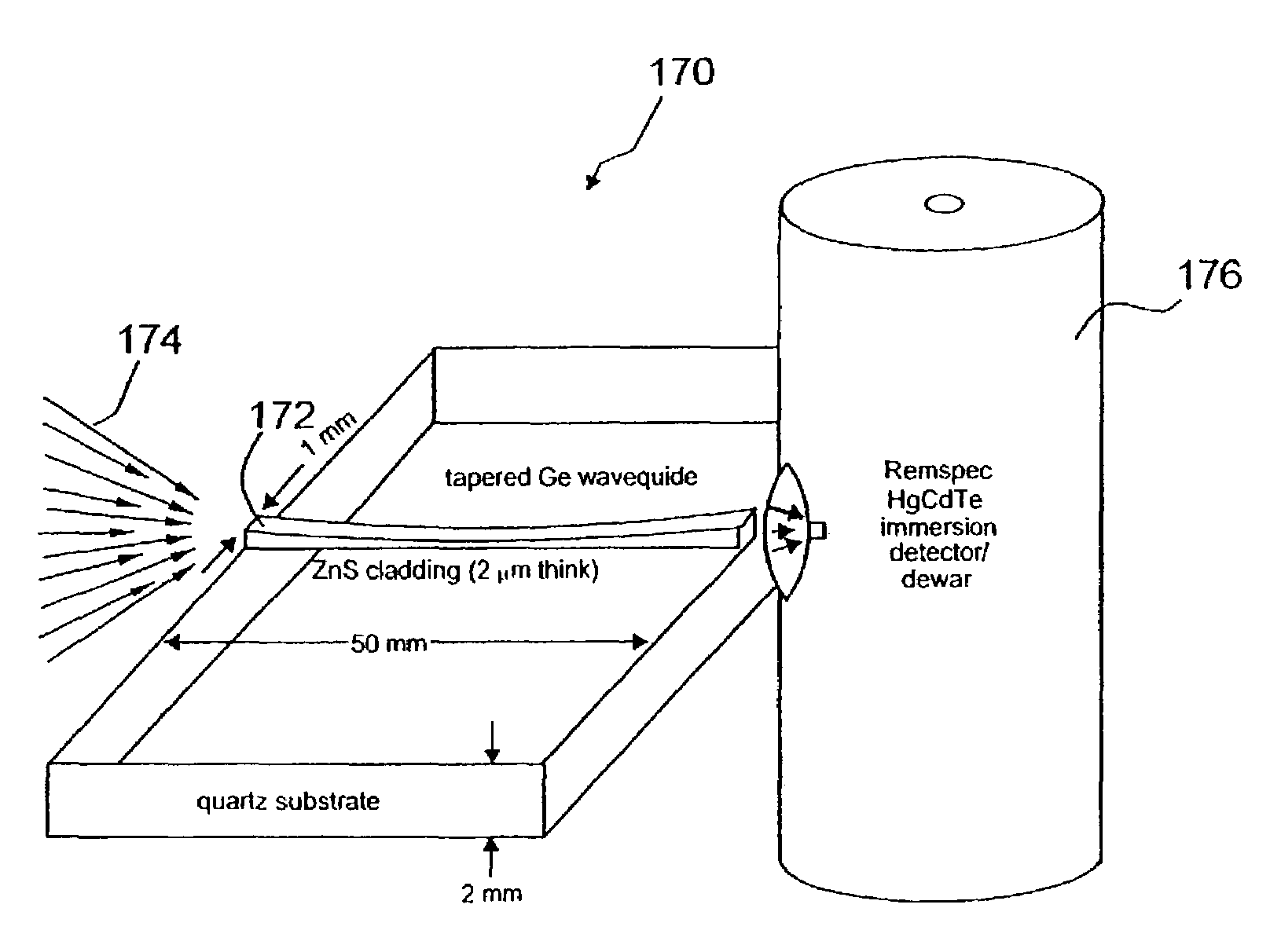
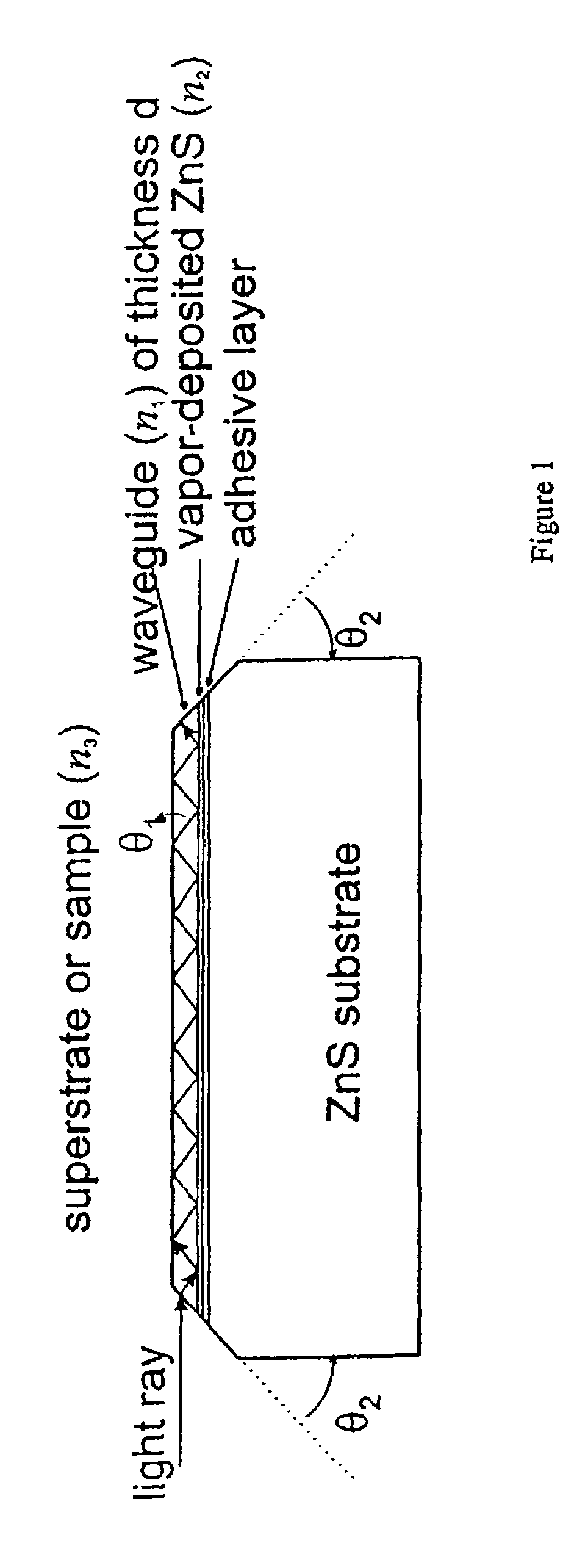
[0035]The waveguides manufactured herein are from germanium prisms, however as the advantages over prior art waveguides are obtained through the science rather than the materials, other elements can be substituted. For example, silicon or cadmium tellurium, will behave similarly, although the mechanical properties of these, and other, materials will require attention to procedures. For example, CdTe is significantly more brittle than Ge and therefore requires additional care during the grinding procedures. When selecting a cladding layer or substrate, the physical properties in relation to one another and to the waveguide material must be taken into account. For example, when selecting a cladding material, the strength of attachment to the waveguide and to the cement / substrate must be considered. Selection of a substrate must take into consideration the rigidity, optical transparency in the UV and the ability to reach a high degree of flatness in surface polish. The Ge / ZnS / quartz co...


PUM

PropertyMeasurementUnit
thicknessaaaaaaaaaa
thicknessaaaaaaaaaa
diameteraaaaaaaaaa

Abstract

Miniature planar IR waveguides of thickness 30–50 μm, consisting of 12-mm long, 2-mm wide strips of Ge supported on ZnS substrates and tapered quasi-tapered waveguides, tapered from a thickness of 1 mm at the ends to a minimum of 1–100 μm at the center, are disclosed. The surface sensitivity is increased as a function of incidence or bevel angle. The tapered waveguide improves the efficiency of the optical coupling both into the waveguide from an FTIR spectrometer, and out of the waveguide onto a small-area IR detector. The tapering makes it possible to dispense with using an IR microscope couple light through the waveguide, enabling efficient coupling with a detector directly coupled to an immersion lens. This optical arrangement makes such thin supported waveguides more useful as sensors, because they can be made quite long (e.g. 50 mm) and mounted horizontally. Furthermore, even with a 20-μm×1-mm cross section, sufficient throughput is obtained to give signal/noise ratios in excess of 1000 over most of the 1000–5000 cm-1 range, with just 2 min of scanning at 8 cm-1 resolution.

Description

CROSS-REFERENCE TO RELATED APPLICATIONS[0001]This application is a continuation-in-part of Ser. No. 09 / 426,055, now U.S. Pat. No. 6,496,636, filed Oct. 25, 1999 and issued on Dec. 17, 2002 which is a continuation-in-part of Ser. No. 08 / 874,711, now U.S. Pat. No. 5,980,831, filed Jun. 13, 1997 and issued Jun. 13, 1997. The present application further claims the benefits under 35 U.S.C. 119(e) of copending provisional patent application Ser. No. 60 / 106,132, filed Oct. 29, 1998. This application incorporates by reference, as though recited in full, the disclosure of parent U.S. Pat. Nos. 6,496,636 and 5,980,831 and copending provisional patent application Ser. No. 60 / 106,132.GOVERNMENT GRANTS[0002]This work was supported by NSF grants MCB-9722887 and MCB-9406681 to Mark S. Braiman.BACKGROUND OF THE INVENTION[0003]The development of mid-infrared (IR) waveguides has been driven by their use as remote or small-sample-size chemical sensors for surface sensitive spectroscopy. Such waveguide...

Claims


Application Information

Patent Timeline
Patent Type & Authority Patents(United States)
IPC IPC(8): B32B37/00G02B6/10G01N21/55G02B6/12G02B6/122G02B6/42
CPCG01N21/552G02B6/42G02B6/1228G01N21/7703G02B2006/12195
Inventor PLUNKETT, SUSAN E.STONE, JAMES J.BRAIMAN, MARK STEPHEN
Owner PLUNKETT SUSAN E
Why Eureka
Try Eureka