MOS linear region impedance curvature correction

a technology of linear region and impedance curvature, which is applied in the direction of amplifiers with field-effect devices, pulse techniques, baseband system details, etc., can solve the problems of increasing system cost and component count, not being able to meet tight impedance specifications, and many non-analog cmos fabrication processes that do not have precision resistors available, etc. , to achieve the effect of tight impedance control, increased output impedance, and greater linearity

Active Publication Date: 2007-10-16
MICRON TECH INC
View PDF11 Cites 6 Cited by
  • Summary
  • Abstract
  • Description
  • Claims
  • Application Information

AI Technical Summary

Benefits of technology

[0027]The present disclosure describes a system and method to correct or cancel MOS linear region impedance curvature. The linear region curvature correction may be obtained by using two MOS transistors in the pad driver / buffer and operating the transistors so as to proportionately increase output impedance of one of the transistors when the output impedance of the other decreases, and vice versa. A linear pad impedance may be maintained over a range of Vpad values, while also maintaining the Vgs supplied to pad driver transistors at its maximum possible value to obtain greater linearity. The approach of the present disclosure relaxes the requirements on the voltage / current references used in the MOS pad drivers and makes tight impedance control possible, especially in a situation where the MOS fabrication process (typically all currently used processes) does not have available an internal precision resistor with reasonably well controlled value. Thus, PVT spreads in values of internal or external precision resistors are also accommodated in a MOS driver circuit built according to the teachings of the present disclosure.

Problems solved by technology

A problem with the current precision resistor approach is that many non-analog CMOS fabrication processes do not have precision resistors available.
In such processes, it may not be possible to meet a tight impedance specification with the circuit of FIG. 2.
Unfortunately, there are some disadvantages with this technique: (1) This technique requires external components and increases system cost and component count.
(3) Even with an external precision resistor, it may not be possible to meet a tight low impedance specification (e.g., under USB2.0 as discussed above with reference to FIG. 1) because of the need to make transistor M1 inordinately large in size (as can be seen from equations (1) and (2) above).
However, the disadvantages of this digital calibration technique are: (1) When it is not possible to drive Vgs to a high value (>>Vds(max) in the Vpad region of interest), then the linear region impedance curvature of transistor M1 (14) can still be very significant.
The addition of an entire third pad for just impedance control may not be desirable.
Impedance updating may not be done safely during data transmission because it could cause major discontinuities in the rise / fall in voltage / current characteristics of the transmitting pad.
This may cause the overall system to fail.
However, there may be no clear “gap” in the transmission protocol and, hence, choosing such “update gap” may pause an additional problem for the system designer.
Such “update gaps” may be defined in the data protocol; however, that is not the case for USB2.0.
However, the disadvantages of the classical analog solution are: (1) Similar to digital trimming, the analog approach trims the pad impedance for one value of Vpad only.
(2) The use of a properly-biased, scaled replica pad may require very tight control of voltage and current references because of the existence of MOS linear region impedance curvature.

Method used


Image

  • MOS linear region impedance curvature correction
  • MOS linear region impedance curvature correction
  • MOS linear region impedance curvature correction

Examples


Embodiment Construction

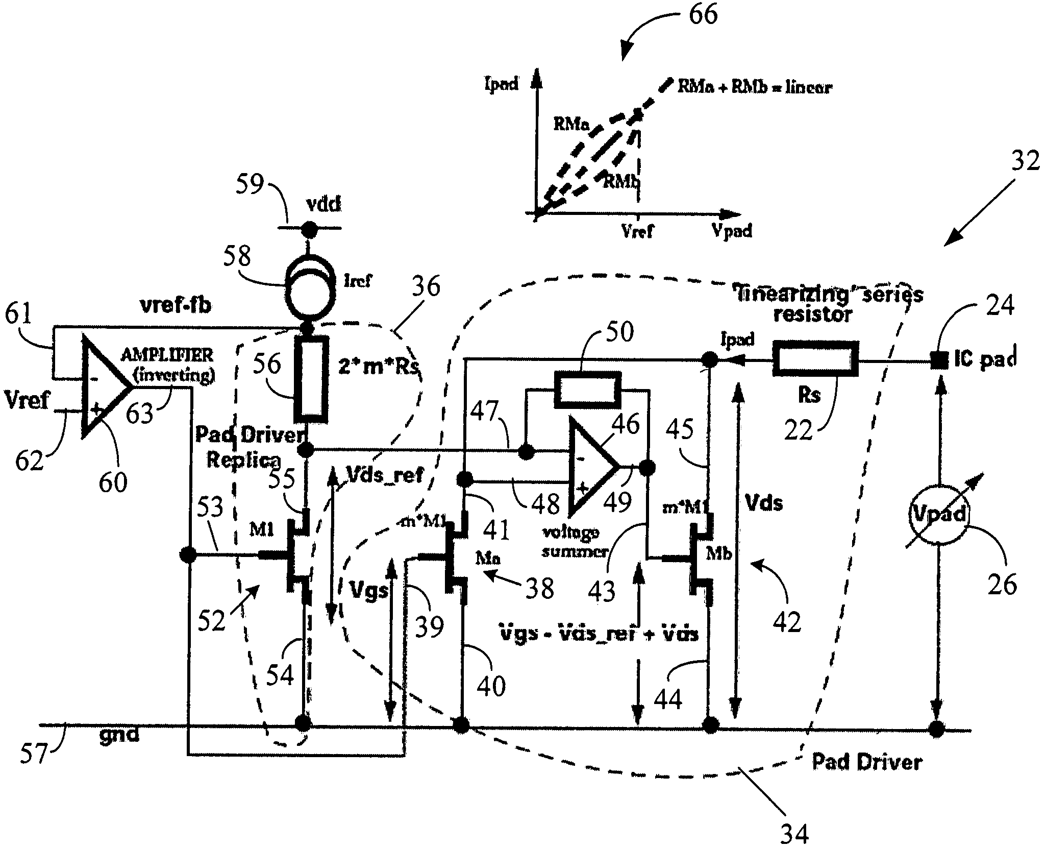
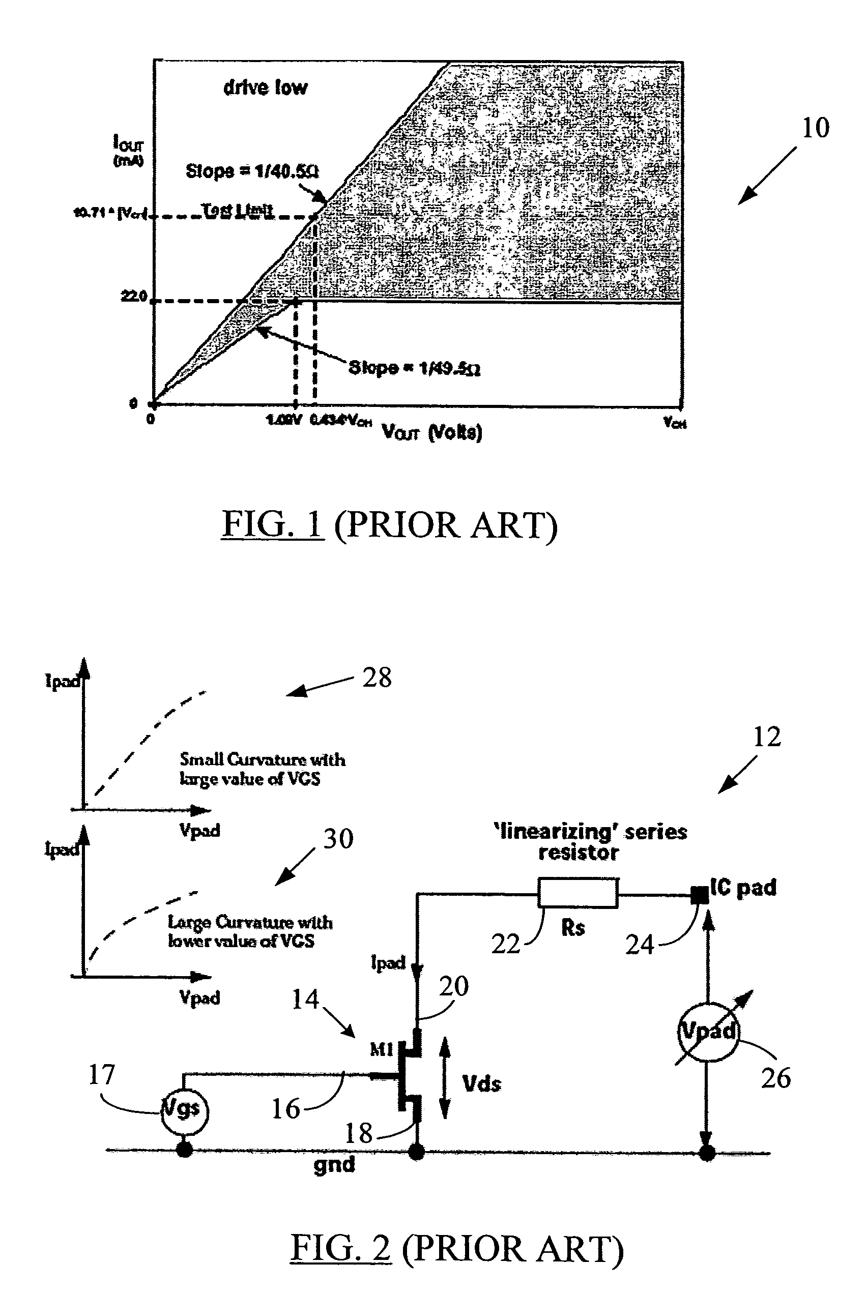
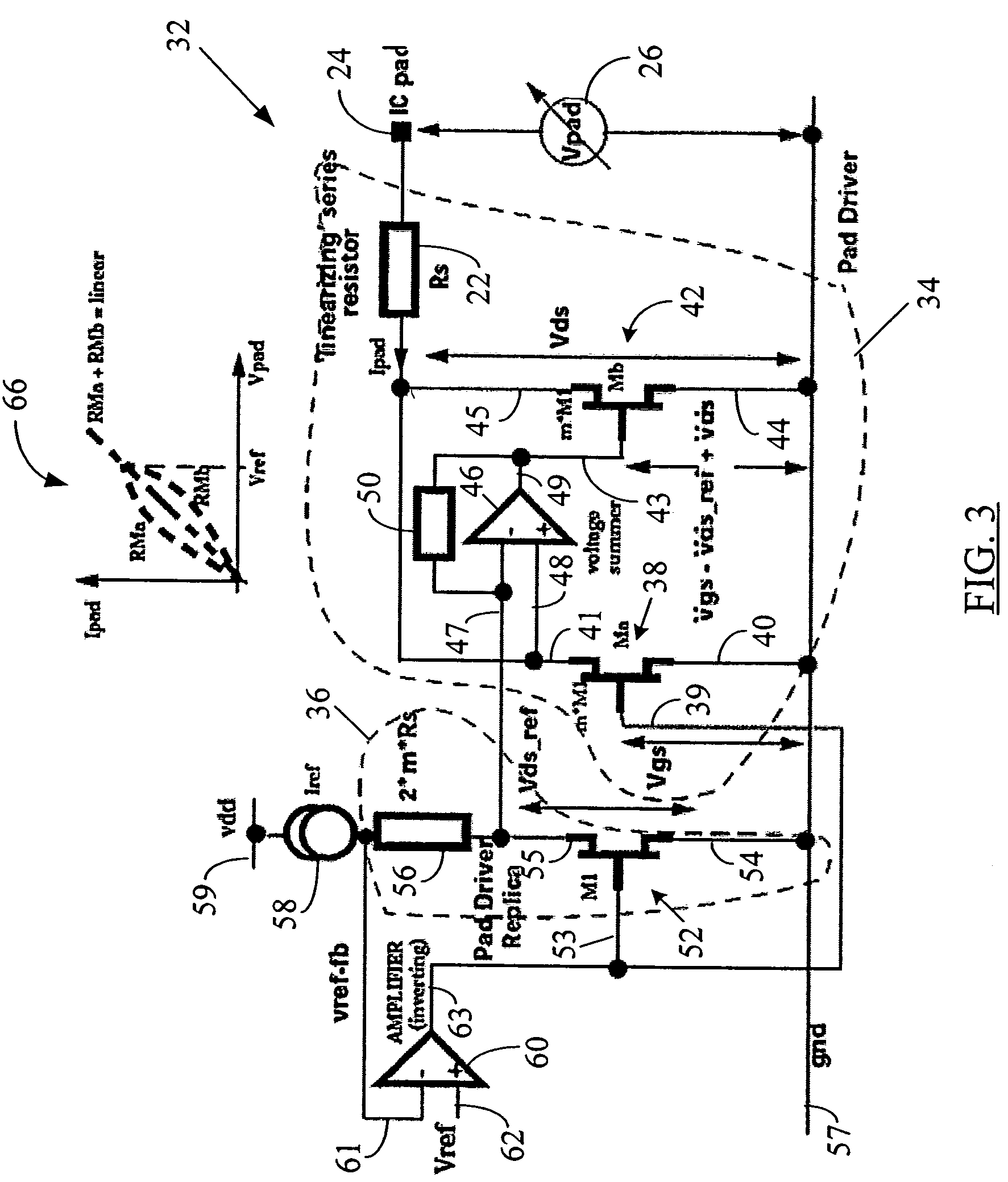
[0049]Reference will now be made in detail to certain embodiments of the present disclosure, examples of which are illustrated in the accompanying drawings. It is to be understood that the figures and descriptions of the present disclosure included herein illustrate and describe elements that are of particular relevance to the present disclosure, while eliminating, for the sake of clarity, other elements found in typical pad drivers or buffers. It is noted at the outset that the terms “connected”, “coupled,”“connecting,”“electrically connected,” etc., are used interchangeably herein to generally refer to the condition of being electrically connected. Further, a terminal is considered “held” at a specific potential when appropriate voltage (e.g., ground potential, reference voltage, supply voltage, etc.) is available at that terminal. The terms “supply” or “provide” are also used interchangeably to refer to electrically supplying or providing a voltage or current to a circuit element...


PUM


Abstract

A system and method to correct or cancel MOS linear region impedance curvature employing an analog solution to trim out the MOS linear region impedance curvature while accommodating PVT spreads in values of internal or external precision resistors. The linear region curvature correction may be obtained by using two MOS transistors in the pad driver / buffer and operating the transistors so as to proportionately increase output impedance of one of them when the output impedance of the other decreases, and vice versa. A linear pad impedance may be maintained over a range of Vpad values, while also maintaining the Vgs supplied to pad driver transistors at its maximum possible value to obtain greater linearity. The approach of the present disclosure relaxes the requirements on the voltage / current references used in the MOS pad drivers and makes tight impedance control possible, especially in a situation where the MOS fabrication process (typically all currently used processes) does not have available an internal precision resistor with a reasonably well controlled value.

Description

BACKGROUND[0001]1. Field of the Disclosure[0002]The present disclosure broadly relates to pad impedance in MOS (Metal Oxide Semiconductor) driver circuits and, more particularly, to an apparatus and method to correct MOS linear region impedance curvature.[0003]2. Brief Description of Related Art[0004]The high speed I / O standards governing data transfers between two high speed electronic devices require a tight control of output impedance of a device driver or buffer circuit in such devices. In modern I / O standards, the output impedance is required to be controlled to a nominal value + / − some percentage error or variation. For example, FIG. 1 illustrates an exemplary pad impedance specification 10 under USB2.0 (Universal Serial Bus version 2.0) for a low impedance driver circuit. An example of a low impedance drive unit is a USB1.1 (Universal Serial Bus version 1.1) buffer circuit within a USB2.0 PHY (Physical Layer) device. The specifications mandated in the chart in FIG. 1 may appl...

Claims


Application Information

Patent Timeline
Patent Type & Authority Patents(United States)
IPC IPC(8): H03K17/16H03F1/32H03K19/003H04L25/02H04L25/12
CPCH03F1/32H03F1/3205H03F3/16H04L25/12H03K19/00384H04L25/028H03K17/162H03K19/018571H04L25/0278
Inventor BALES, TIM J.
Owner MICRON TECH INC
Why Eureka
Try Eureka