Integrated platform for passive optical alignment of semiconductor device with optical fiber

a technology of integrated platform and optical fiber, which is applied in the field of packaging optoelectronic components, can solve the problems of high cost of manufacturing fiber optic interfaces, insensitive long-range communication systems, and high manufacturing cost of optical fiber interfaces, and achieves low cost, reduced alignment tolerances, and effective demagnification

Inactive Publication Date: 2007-10-30
CLOUD LIGHT TECH LTD
View PDF11 Cites 36 Cited by
  • Summary
  • Abstract
  • Description
  • Claims
  • Application Information

AI Technical Summary

Benefits of technology

[0016]According to one embodiment of the invention, a single platform is provided that reduces alignment tolerances through its integrated features. These features include a mirror to deflect a light beam from an attached source transmitter toward an optical fiber, an integrated focusing lens between the mirror and the fiber with an effective demagnification image at the fiber, and a v-shaped groove structure for receiving the optical fiber in the same platform. The platform may be manufactured inexpensively, such as by transfer / injection molding, grinding or polishing of glass and plastic material, depending on the particular application. The same principles may be applied where photo-detectors are used for receiving the light beam instead of transmitting the light beam.
[0019]According to the present invention, 1) the working distances between the platform and optical fiber are extended; 2) the beam profile is adjusted into symmetrical form by a focusing lens; and 3) the tolerances for passive alignment are relaxed in x and y dimensions as compared to conventional techniques. These features reduce the cost of manufacturing optical packages.

Problems solved by technology

However, optical fiber interfaces to electronic and optical networks are expensive to manufacture because of the difficulty associated with mounting laser transmitting and receiving devices onto substrates and aligning them with separately mounted optical fibers.
Long haul communications systems are also relatively price insensitive.
However, the high cost of manufacturing fiber optic interfaces has been a barrier that has slowed the penetration of fiber optic technology into local metropolitan area communication systems and other markets.
Because of the small dimensions of optical fiber cores, aligning optical fibers with laser transmitting and receiving devices, which have aperture sizes that vary from approximately 2 to 10 microns, is difficult.
The problem is particularly acute when devices are aligned with single mode fibers because of their small core diameter.
This is because of the tight tolerances and limitations required to optically couple a laser beam between the aperture of a laser transmitting or receiving device and the small core of a single mode fiber.
The problem is exacerbated by the use of inexpensive though desirable materials for the platform, which may inherently have manufacturing tolerances that are difficult to control.
Without modification, the tolerance offered by flip chip bonding of approximately 1 micron does not meet the required tolerance of 0.5 microns required for coupling an optical beam from a mounted device into a single-mode fiber.
The flat, slanted reflecting surface of these designs has several fundamental drawbacks, including: (i) the limited working distance defined as the distance between the device and the optical fiber; (ii) the failure to compensate the beam profile in the case of diode laser coupling; and (iii) high aggregate placement tolerances between the opto-electronic device and the fiber.
However, this coupling scheme may not always be possible, as it is often limited by physical constraints.
These issues greatly reduce or prohibit the use of this platform for the single-mode or multi-mode laser packaging using semiconductor diode lasers.
However, single crystal silicon is very expensive, compared to glass and plastics.
However, these waveguides have not conventionally provided a sitting platform for a laser transmitting or receiving device.
Thus, active alignment has been needed to place and align the separately packaged device with the waveguide, which is labor intensive and costly.
This adds to the cost of the assembly.
To a lesser degree, the handling of many small mechanical components of hundreds of micrometers to a few millimeters in size and the sealing in a hermetic environment also adds to the cost of packaging.
However, the emergence of the short reach metro / access markets, which is the next growth area in photonics, increases the need for low-cost packaging because these markets are extremely price-sensitive.

Method used


Image

  • Integrated platform for passive optical alignment of semiconductor device with optical fiber
  • Integrated platform for passive optical alignment of semiconductor device with optical fiber
  • Integrated platform for passive optical alignment of semiconductor device with optical fiber

Examples


Embodiment Construction

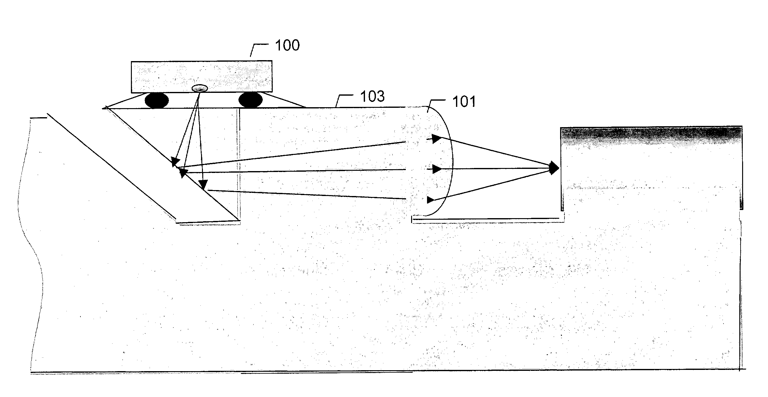
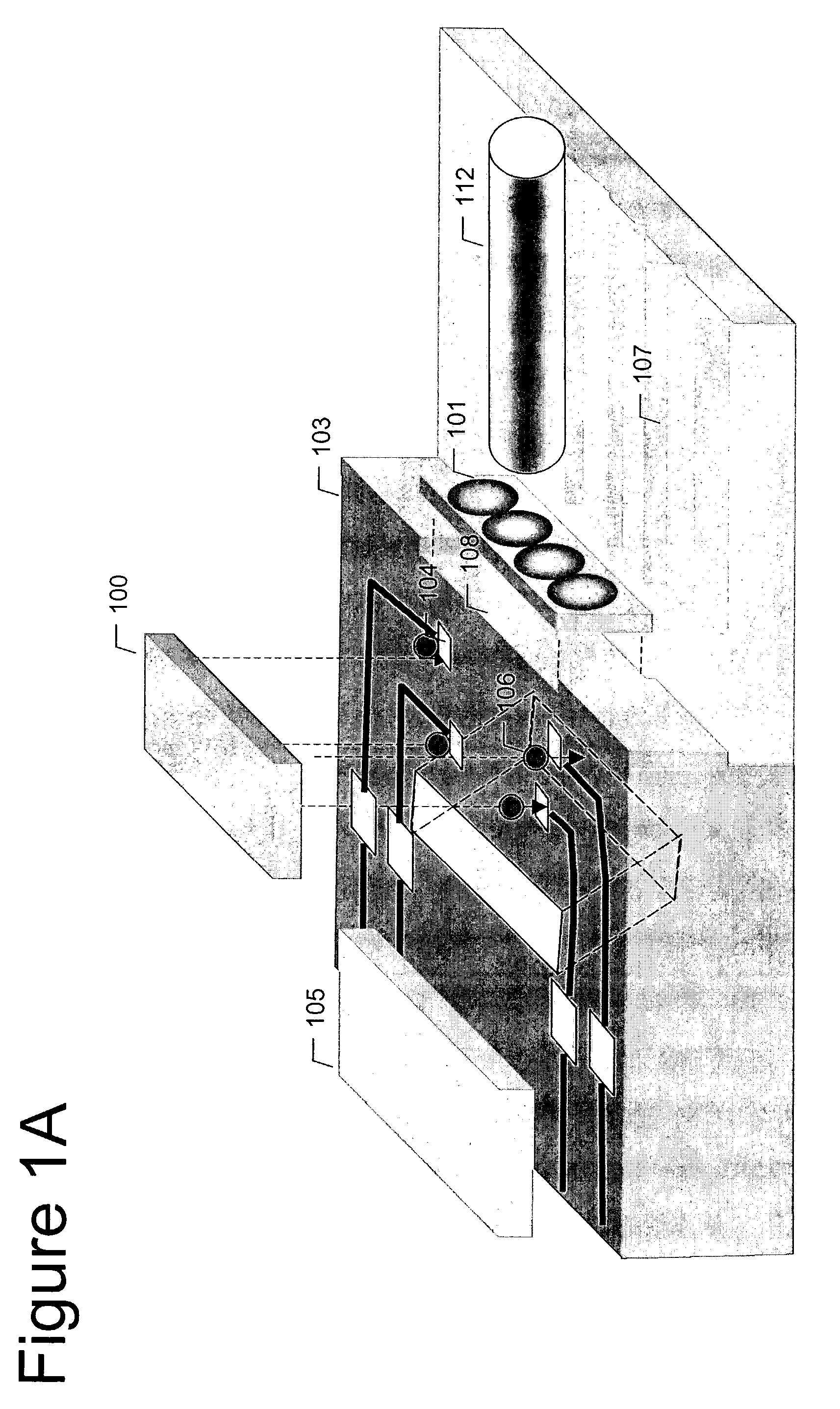
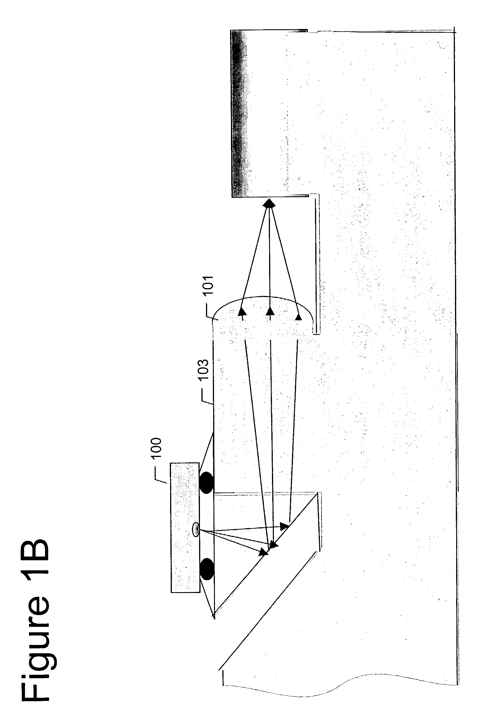
[0039]According to one embodiment of the invention, a single platform is provided that reduces alignment tolerances through its integrated features. These features include a 45-degree mirror to deflect a laser beam from a vertical cavity surface emitting laser (VCSEL) transmitter toward an optical fiber, a focusing lens between the mirror and the fiber with an effective demagnification image at the fiber, and a v-shaped groove structure for receiving the optical fiber in the same platform. The platform may be manufactured inexpensively, such as by transfer / injection molding, grinding or polishing of glass and plastic material, depending on the particular application. The same principles may be applied where photodetectors are used for receiving the laser instead of transmitting the laser.

[0040]FIG. 1A depicts a three dimensional view of an integrated platform according to an embodiment of the present invention showing pads and interconnections for electrically and optically coupling...


PUM


Abstract

A platform for converting a signal between optical and electrical form and vice versa is provided. The platform includes a dielectric mount, a semiconductor light source and optical fibers. Some of these components are fabricated separately and then brought together in an integrated assembly together with a focusing lens. The platform permits the self-alignment of the optical fibers in a flip-chip vertical cavity surface emitting laser (VCSEL) array module package. The self-alignment of the optical fibers is achieved by the engineering of the geometrical dimensions of the platform. The techniques may be used to form large-scale integrated opto-electronic circuits and switching networks.

Description

CROSS-REFERENCE TO RELATED APPLICATION[0001]This application claims priority to provisional patent application No. 60 / 363,880 filed Mar. 14, 2002.FIELD OF THE INVENTION[0002]The present invention relates to packaging opto-electronic components and, more particularly, to an integrated platform for facilitating the physical and optical coupling of light transmitting and receiving devices to optical fibers.BACKGROUND OF THE INVENTION[0003]Optical fiber technology is well suited for communications applications because optical fibers have a wide transmission bandwidth and relatively low attenuation. However, optical fiber interfaces to electronic and optical networks are expensive to manufacture because of the difficulty associated with mounting laser transmitting and receiving devices onto substrates and aligning them with separately mounted optical fibers. For this reason, optical fiber technology has been widely implemented in long haul communication systems where the interfaces are r...

Claims


Application Information

Patent Timeline
Patent Type & Authority Patents(United States)
IPC IPC(8): G02B6/30G02B6/42
CPCG02B6/4204G02B6/4214G02B6/4231G02B6/4249G02B6/4232G02B6/423
Inventor LAM, DENNISHO, FLORALAM, S. K.TONG, FRANKLIN
Owner CLOUD LIGHT TECH LTD
Why Eureka
Try Eureka