Light emitting element including a barrier layer and a manufacturing method thereof

a technology barrier layers, which is applied in the direction of discharge tubes/lamp details, discharge tubes luminescnet screens, electric discharge lamps, etc., can solve the problems of high power consumption, inability to obtain sufficient luminance, and difficulty in solving the stability problems of light emitting elements, so as to improve the efficiency of hole injection into the hole injection layer and enhance the light emission characteristics

Inactive Publication Date: 2007-11-06
SEMICON ENERGY LAB CO LTD
View PDF37 Cites 39 Cited by
  • Summary
  • Abstract
  • Description
  • Claims
  • Application Information

AI Technical Summary

Benefits of technology

[0009]The present invention has been made in view of the above problems and it is an object of the invention to provide a light emitting element with high stability, good light emission characteristics, and high luminance with low power consumption.
[0012]As to a light emitting element according to the invention, a hole injection electrode is formed with a light transmitting conductive oxide layer containing silicon or silicon oxide; a hole injection layer or a hole transport layer is formed of an organic compound, and an insulating or semi-insulating barrier layer which improves hole injection efficiency is provided between the hole injection electrode and the hole injection layer or hole transport layer.
[0014]As to a light emitting element according to the invention, a hole injection electrode is formed with a light transmitting conductive oxide layer containing silicon or silicon oxide; a hole injection layer or a hole transport layer is formed of an organic compound; and an insulating or semi-insulating barrier layer which layer improves hole injection efficiency is provided to prevent the hole injection electrode and the hole injection layer or hole transport layer from contacting each other.
[0018]The invention includes the steps of: forming an insulating or semi-insulating barrier layer which improves hole injection efficiency, on the surface of a hole injection electrode formed with a light transmitting conductive oxide layer containing silicon or silicon oxide; and forming a hole injection layer or a hole transport layer, either of which is formed of an organic compound over the barrier layer.
[0022]As to the light emitting element configured as above, the hole injection electrode and the hole injection layer does not directly contact each other. Accordingly, the original work function of the hole injection electrode can be acquired, and the efficiency of hole injection into the hole injection layer is improved; thus, light emission characteristics can be enhanced.

Problems solved by technology

However, in the case of a light emitting device having a conventional structure in which an organic compound is stacked over an electrode formed of an inorganic compound, sufficient luminance can not be obtained.
Further, such a light emitting element has problems to be solved with respect to stability such as high power consumption and short half life of luminance.

Method used


Image

  • Light emitting element including a barrier layer and a manufacturing method thereof
  • Light emitting element including a barrier layer and a manufacturing method thereof
  • Light emitting element including a barrier layer and a manufacturing method thereof

Examples


embodiment 1

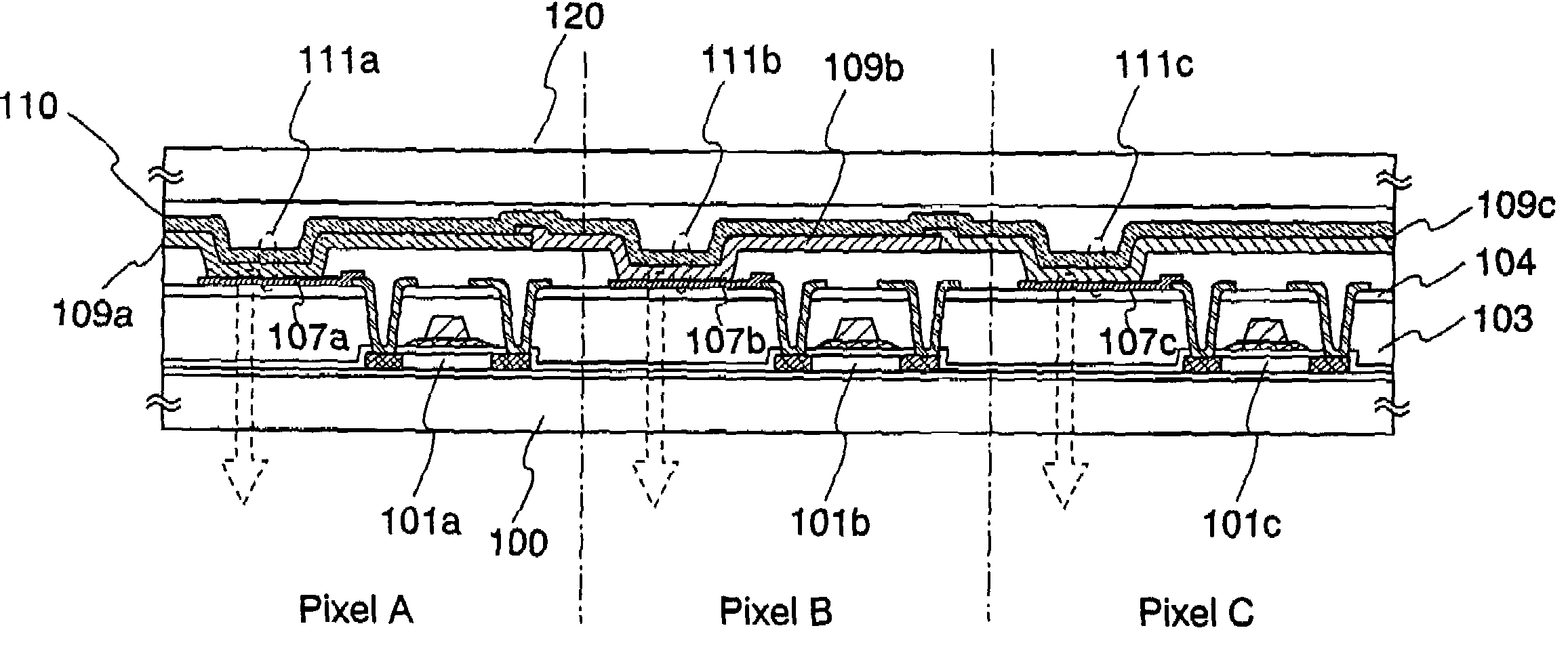
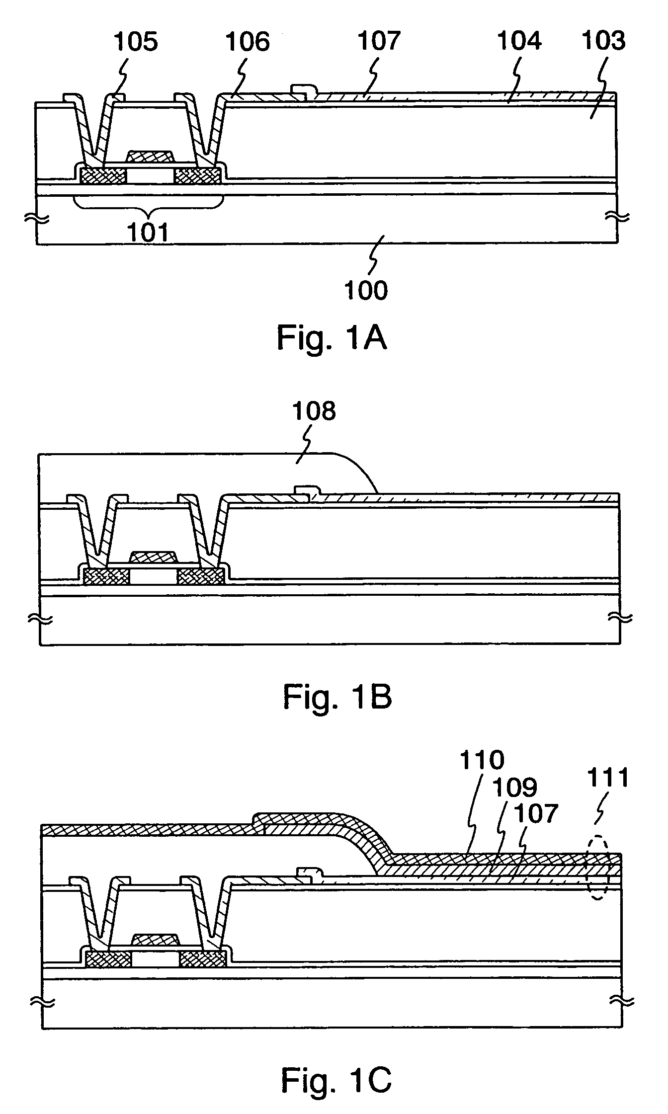
[0087]A light emitting device manufactured according to this embodiment will be described with reference to FIG. 1.

[0088]A first interlayer insulating film 103 is formed with silicon oxynitride films. Specifically, the first interlayer insulating film 103 is formed by laminating a 30-nm-thick first silicon oxynitride film and a 200-nm-thick second silicon oxynitride film by plasma CVD to a thickness of 230 nm in total. The second interlayer insulating film 104 is formed with a silicon nitride film with a thickness of 100 nm by sputtering using silicon as a target.

[0089]A hole injection electrode 107 is formed with an ITSO film to a thickness of 110 nm by sputtering using a target (934 mm×158 mm) having a composition ratio of 85 wt % indium oxide (In2O3), 10 tin oxide (SnO2), 5 wt % silicon oxide (SiO2), and a sputtering gas of 120 sccm Ar and 5 sccm oxygen at a pressure of 0.26 Pa and with a DC electrical power of 3.3 kW. The hole injection electrode 107 is formed by patterning the ...


PUM


Abstract

According to the invention, an insulating or semi-insulating barrier layer which has a thickness where a tunnel current can flow through is provided between a hole injection electrode and an organic compound layer with hole transport characteristics (a hole injection layer or a hole transport layer). Specifically, a thin insulating or semi-insulating barrier layer which contains silicon or silicon oxide; silicon or silicon oxide and a light transmitting conductive oxide material; or silicon or silicon oxide, a light transmitting conductive oxide material, and carbon may be provided between a light transmitting conductive oxide film formed of a light transmitting conductive oxide material, such as ITO and a hole injection layer containing an organic compound.

Description

BACKGROUND OF THE INVENTION[0001]1. Field of the Invention[0002]The present invention relates to a light emitting element using an electroluminescent material. Specifically, the invention relates to an element structure of a light emitting element in which a pair of electrodes and an organic compound layer therebetween are stacked.[0003]2. Description of the Related Art[0004]A light emitting element in which electroluminescence (hereinafter also referred to as EL) is produced by using a pair of electrodes sandwiching mainly a layer containing an organic compound has been attracting attention. The light emitting element uses a phenomenon below; a hole injected from one electrode and an electron injected from the other electrode recombine to excite luminescence center, thereafter light is emitted when luminescence center back to a ground state. That is, the light emitting element is formed so that organic compounds with different carrier transport characteristics are stacked between a...

Claims


Application Information

Patent Timeline
Patent Type & Authority Patents(United States)
IPC IPC(8): H01J63/04H01L33/00H01L51/50H05B33/10H05B33/12H05B33/14H05B33/20H05B33/22
CPCH01L51/5088H01L27/3244H01L51/5237H10K59/12H10K50/17H10K50/846H10K50/8426H10K50/15H10K50/84
Inventor SAKATA, JUNICHIROMURAKAMI, MASAKAZUMORIYA, KOJIOIKAWA, YOSHIAKIASAMI, TAKETOMIOHTANI, HISASHI
Owner SEMICON ENERGY LAB CO LTD
Why Eureka
Try Eureka