Nitride semiconductor device such as transverse power FET for high frequency signal amplification or power control

a technology of transverse power fet and semiconductor, which is applied in the manufacture of semiconductor/solid-state devices, semiconductor devices, electrical equipment, etc., can solve the problems of deteriorating state of gate insulating film and semiconductor layer interface, and difficulty in achieving excellent interface between gate insulating film and semiconductor layer

Inactive Publication Date: 2007-12-04
KK TOSHIBA
View PDF18 Cites 157 Cited by
  • Summary
  • Abstract
  • Description
  • Claims
  • Application Information

AI Technical Summary

Problems solved by technology

In a combination of the alumimum oxide (Al2O3) with the aluminum gallium nitride / gallium nitride (AlGaN / GaN) heterostructure, however, it is difficult to achieve an excellent interface between the gate insulating film and the semiconductor layer.
However, since the silicon nitride (SiN) film is considerably different in thermal expansion coefficient from the aluminum oxide (Al2O3) film or the aluminum gallium nitride / gallium nitride (AlGaN / GaN) layer positioned above or below, there arises such a problem that a state of an interface between the gate insulating film and the semiconductor layer deteriorates due to thermal treatment process.

Method used


Image

  • Nitride semiconductor device such as transverse power FET for high frequency signal amplification or power control
  • Nitride semiconductor device such as transverse power FET for high frequency signal amplification or power control
  • Nitride semiconductor device such as transverse power FET for high frequency signal amplification or power control

Examples


first embodiment

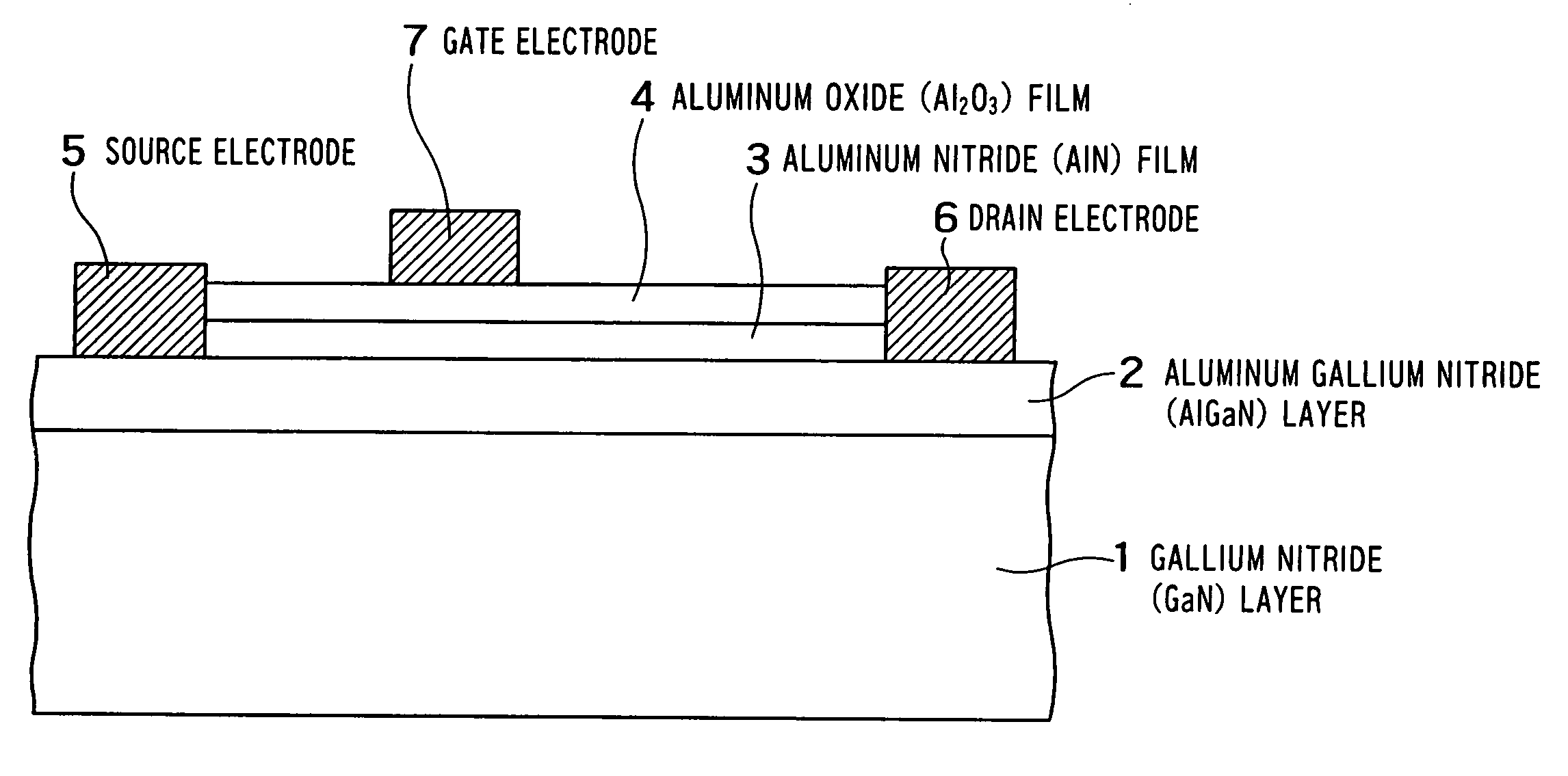
[0038]FIG. 1 is a sectional view illustratively showing a structure of a nitride semiconductor device according to the invention.

[0039]A nitride semiconductor device according to the first embodiment of the invention includes a non-doped gallium nitride (GaN) layer 1 serving as a channel layer, a non-doped aluminum gallium nitride (AlGaN) layer 2 which is formed on the gallium nitride (GaN) layer 1 to serve as a barrier layer, an aluminum nitride (AlN) film 3 which is formed on the aluminum gallium nitride (AlGaN) layer 2 to serve as a gate insulating film lower layer, an aluminum oxide (Al2O3) film 4 which is formed on the aluminum nitride (AlN) film 3 to serve as a gate insulating film upper layer, a source electrode 5 and a drain electrode 6 which are respectively formed so as to be electrically connected to the aluminum gallium nitride (AlGaN) layer 2 to serve as first and second main electrodes, and a gate electrode 7 which is formed on the aluminum oxide (Al2O3) film 4 to serv...

second embodiment

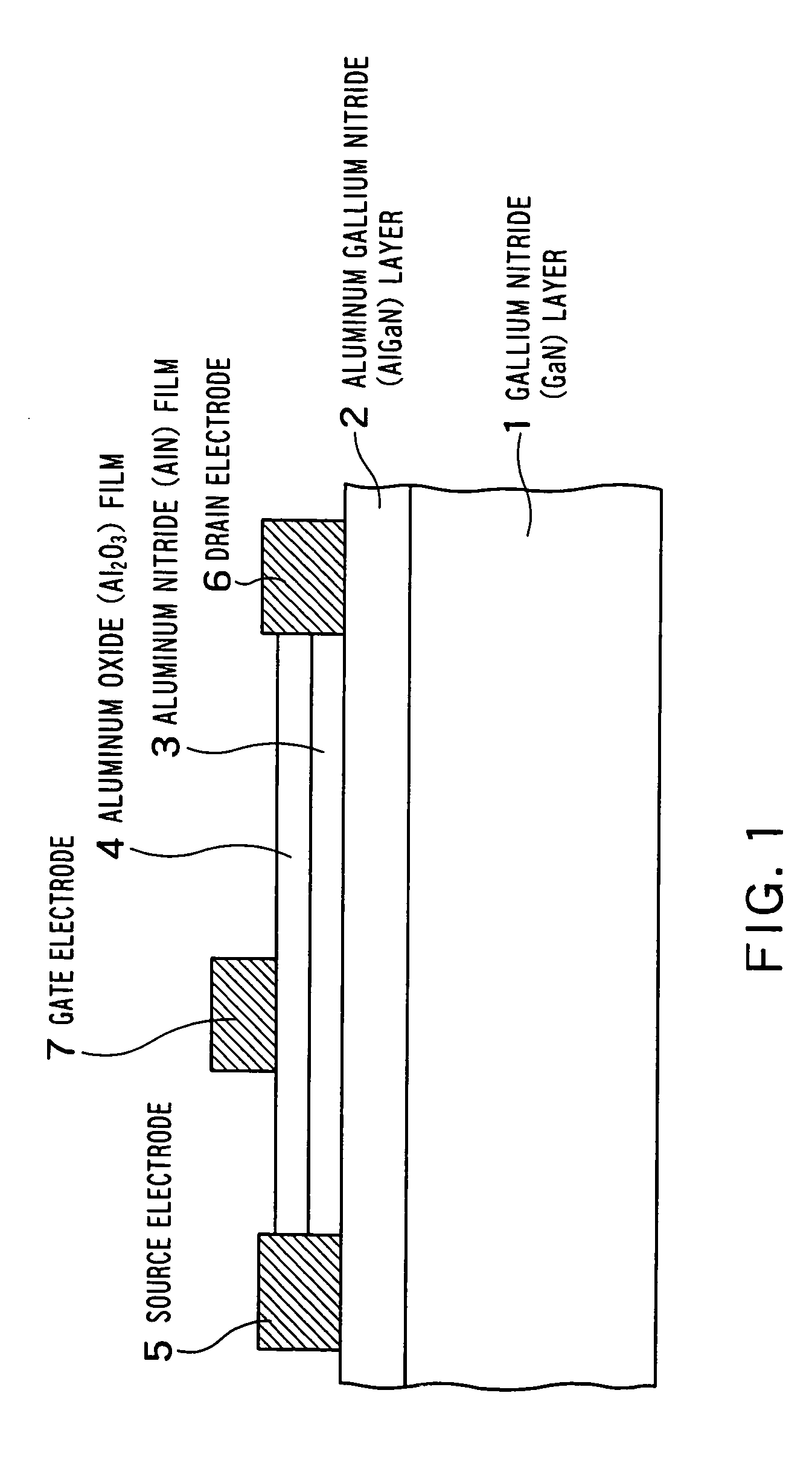
[0050]FIG. 2 is a sectional view illustratively showing a structure of a nitride semiconductor device according to the invention.

[0051]A nitride semiconductor device according to the second embodiment of the invention includes a non-doped gallium nitride (GaN) layer 1 serving as a channel layer, a non-doped aluminum gallium nitride (AlGaN) layer 2 which is formed on the gallium nitride (GaN) layer 1 to serve as a barrier layer, an aluminum nitride (AlN) film 3 which is formed on the aluminum gallium nitride (AlGaN) layer 2 to serve as a gate insulating film lower layer, an aluminum oxide (Al2O3) film 4 which is formed on the aluminum nitride (AlN) film 3 to serve as a gate insulating film upper layer, a source electrode 5 and a drain electrode 6 which are respectively formed so as to be electrically connected to the aluminum gallium nitride (AlGaN) layer 2 to serve as first and second main electrodes, and a gate electrode 7 which is formed on the aluminum oxide (Al2O3) film 4 to ser...

third embodiment

[0056]FIG. 3 is a sectional view illustratively showing a structure of a nitride semiconductor device according to the invention.

[0057]A nitride semiconductor device according to the third embodiment of the invention includes a non-doped gallium nitride (GaN) layer 1 serving as a channel layer, a non-doped aluminum gallium nitride (AlGaN) layer 2 which is formed on the gallium nitride (GaN) layer 1 to serve as a barrier layer, an aluminum nitride (AlN) film 3 which is formed on the aluminum gallium nitride (AlGaN) layer 2 to serve as a gate insulating film lower layer, an aluminum oxide (Al2O3) film 4 which is formed on the aluminum nitride (AlN) film 3 to serve as a gate insulating film upper layer, a source electrode 5 and a drain electrode 6 which are respectively formed so as to be electrically connected to the aluminum gallium nitride (AlGaN) layer 2 to serve as first and second main electrodes, and a gate electrode 7 which is formed on the aluminum oxide (Al2O3) film 4 to serv...


PUM

PropertyMeasurementUnit
conductive typeaaaaaaaaaa
electric fieldaaaaaaaaaa
breakdown voltageaaaaaaaaaa

Abstract

A nitride semiconductor device according to one embodiment of the present invention includes: a non-doped first aluminum gallium nitride (AlxGa1-xN (0≦x≦1)) layer which is formed as a channel layer; a non-doped or n type second aluminum gallium nitride (AlyGa1-yN (0≦y≦1, x <y)) layer which is formed on the first aluminum gallium nitride layer as a barrier layer; an aluminum nitride (AlN) film which is formed on the second aluminum gallium nitride layer as a gate insulating film lower layer; an aluminum oxide (AL2O3) film which is formed on the aluminum nitride film as a gate insulating film upper layer; a source electrode and a drain electrode which are formed as first and second main electrodes to be electrically connected to the second aluminum gallium nitride layer, respectively; and a gate electrode which is formed on the aluminum oxide film as a control electrode.

Description

CROSS REFERENCE TO RELATED APPLICATION[0001]The subject application is related to subject matter disclosed in Japanese Patent Application No. 2004-207409 filed on Jul. 14, 2004 in Japan to which the subject application claims priority under Paris Convention and which is incorporated herein by reference.BACKGROUND OF THE INVENTION[0002]1. Field of the Invention[0003]The present invention relates to a nitride semiconductor device, and in particular to a transverse power FET which is used for high frequency signal amplification, power control or the like.[0004]2. Related Background Art[0005]Since an electronic device including a aluminum gallium nitride / gallium nitride (AlGaN / GaN) heterostructure has a critical electric field higher than that in a conventional electronic device which includes gallium arsenide (GaAs) or silicon (Si) as main material and is used for high frequency signal amplification or power control, it allows realization of a high breakdown voltage and high output dev...

Claims


Application Information

Patent Timeline
Patent Type & Authority Patents(United States)
IPC IPC(8): H01L31/0328H01L31/0336H01L31/072H01L31/109H01L21/336H01L21/338H01L29/06H01L29/41H01L29/78H01L29/812
CPCH01L29/1066H01L29/402H01L29/7786H01L29/41725H01L29/432H01L29/517H01L29/404H01L29/2003
Inventor SAITO, WATARUOMURA, ICHIRO
Owner KK TOSHIBA
Why Eureka
Try Eureka