Gallium-nitride based ultraviolet photo detector

a technology of gallium nitride and ultraviolet light, applied in the field of photo detectors, can solve the problems of high operation voltage, high production cost, and fragility of vacuum tubes

Active Publication Date: 2007-12-11
FORMOSA EPITAXY INCORPORATION +1
View PDF2 Cites 24 Cited by
  • Summary
  • Abstract
  • Description
  • Claims
  • Application Information

AI Technical Summary

Benefits of technology

[0008]The present invention provides an epitaxial structure for the GaN-based UV photo detectors so that the limitations and disadvantages from the prior arts can be obviated practically.
[0009]The structure of the GaN-based UV photo detectors comprises, on top of an upper side of a substrate, an n-type contact layer, a light absorption layer, a light penetration layer, and a p-type contact layer, sequentially stacked in this order from bottom to top. All these layers are made of aluminum-gallium-indium-nitride (AlaGabIn1−a−bN, 0≦a,b≦1, a+b≦1) compound semiconducting materials having specific compositions. By varying the Al, Ga, and In composition within these materials, these layers would have the required band gaps, carrier densities, and carrier mobilities. The GaN-based UV photo detectors therefore can be especially sensitive to UV lights having specific wavelengths. On the other hand, these layers can be developed to have compatible lattice constants, avoid the development and accumulation of excessive stress, and contribute to a superior epitaxial structure of the GaN-based UV photo detectors.

Problems solved by technology

Among the three approaches, PMTs have a number of disadvantages such as high production cost, high operation voltage, and the fragility of vacuum tubes.
However, despite their rather superior performance in detecting lights with longer wavelengths such as visible lights and infrared lights, Si-based photo detectors are less sensitive to lights with shorter wavelengths such as the ultraviolet (UV) lights.
One of the major problems to known GaN-based semiconductor devices is that there is often an incompatibility in terms of lattice constants within the GaN-based semiconductor devices' layering structure.
Such discrepancies in the lattice structures develop and accumulate excessive stress, causing an inferior epitaxial structure of the GaN-based semiconductor devices and thereby an unsatisfactory device performance.

Method used


Image

  • Gallium-nitride based ultraviolet photo detector
  • Gallium-nitride based ultraviolet photo detector
  • Gallium-nitride based ultraviolet photo detector

Examples


first embodiment

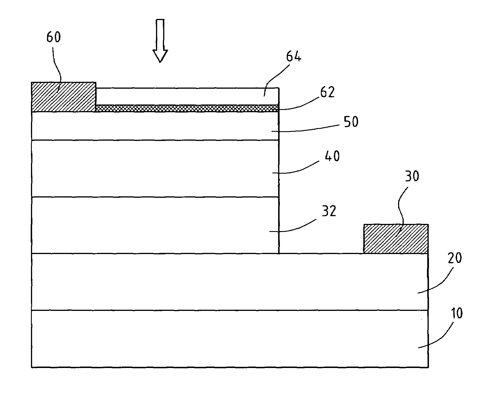
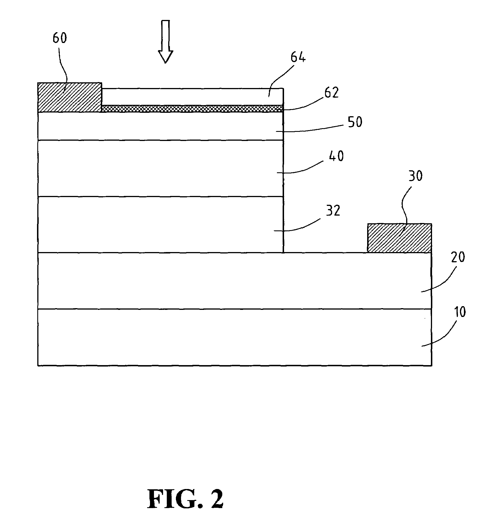
[0018]FIG. 2 is a schematic diagram showing the epitaxial structure of the GaN-based UV photo detector according to the present invention. As shown in FIG. 2, the GaN-based UV photo detector has a substrate 10 made of C-plane, R-plane, or A-plane aluminum-oxide monocrystalline (sapphire), or an oxide monocrystalline having a lattice constant compatible with that of nitride semiconductors. The substrate 10 can also be made of SiC (6H—SiC or 4H—SiC), Si, ZnO, GaAs, or MgAl2O4. Generally, the most common material used for the substrate 10 is sapphire or SiC. An n-type contact layer 20 made of n-type doped AlaGabIn1−a−bN (0≦a,b≦1, a+b≦1) having a specific composition is then formed on an upper side of the substrate 10. The n-type contact layer 20 has a thickness between 3000 Å and 40000 Å and a growing temperature between 700° C. and 1200° C. Then, a light absorption layer 32 made of undoped AlcGadIn1−c−dN (0≦c,d≦1, c+d≦1) having a specific composition is grown on the n-type contact lay...

third embodiment

[0024]FIG. 4 is a schematic diagram showing the epitaxial structure of the GaN-based UV photo detector according to the present invention. As shown in FIG. 4, the present embodiment has an identical structure as in the previous embodiments. The only difference lies in the material used and the structure of the light absorption layer. Within the present embodiment, the light absorption layer 36 has a superlattice structure comprising multiple (≧2) intermediate layers. Each intermediate layer comprises two base layers made of undoped AlpGaqIn1−p−qN and AlrGasIn1−r−sN (0≦p,q,r,s≦1, p+q≦1, r+s≦1) respectively. Each of the base layers has a specific composition, a thickness between 50 Å and 200 Å, and a growing temperature between 700° C. and 1200° C., all independent of other base layers. The light absorption layer 36 has a total thickness between 100 Å and 10000 Å. The superlattice structure of the present embodiment avoids the cracking problem of a single-layered thick film having a h...


PUM


Abstract

A structure for a gallium-nitride (GaN) based ultraviolet photo detector is provided. The structure contains an n-type contact layer, a light absorption layer, a light penetration layer, and a p-type contact layer, sequentially stacked on a substrate from bottom to top in this order. The layers are all made of aluminum-gallium-indium-nitride (AlGaInN) compound semiconductors. By varying the composition of aluminum, gallium, and indium, the layers, on one hand, can achieve the desired band gaps so that the photo detector is highly responsive to ultraviolet lights having specific wavelengths. On the other hand, the layers have compatible lattice constants so that problems associated with excessive stress are avoided and high-quality epitaxial structure is obtained. The structure further contains a positive electrode, a light penetration contact layer, and an anti-reflective coating layer on top of the p-type contact layer, and a negative electrode on the n-type contact layer.

Description

BACKGROUND OF THE INVENTION[0001]1. Field of the Invention[0002]The present invention generally relates to the photo detectors and, more particularly, to the gallium-nitride based ultraviolet photo detectors.[0003]2. The Prior Arts[0004]Currently there are three commonly known approaches to building photo detectors that can convert light signals to electrical signals: photo multipliers (PMTs) based on vacuum tubes; photo detectors made of silicon (Si); and photo detectors made of gallium-nitride (GaN) based compound semiconductors.[0005]Among the three approaches, PMTs have a number of disadvantages such as high production cost, high operation voltage, and the fragility of vacuum tubes. The Si-based photo detectors, on the other hand, are easer to manufacture, less costly in production, and operated with lower voltage. However, despite their rather superior performance in detecting lights with longer wavelengths such as visible lights and infrared lights, Si-based photo detectors ar...

Claims


Application Information

Patent Timeline
Patent Type & Authority Patents(United States)
IPC IPC(8): H01L31/072
CPCB82Y20/00H01L31/03046H01L31/101H01L31/1852H01L31/035236Y02E10/544
Inventor WU, LIANG-WENTU, RU-CHINYU, CHENG-TSANGWEN, TZU-CHICHIEN, FEN-REN
Owner FORMOSA EPITAXY INCORPORATION
Why Eureka
Try Eureka