Optical modulator

a technology of optical modulator and optical bandwidth, applied in the field of structure and operation of optical modulator, can solve the problems of low modulation contrast, low efficiency, and dramatic reduction of optical bandwidth of fabry-pérot structure, and achieve the effect of increasing the reflection

Inactive Publication Date: 2007-12-25
NOKIA SOLUTIONS & NETWORKS OY +1
View PDF7 Cites 87 Cited by
  • Summary
  • Abstract
  • Description
  • Claims
  • Application Information

AI Technical Summary

Problems solved by technology

In general a major problem with surface-normal modulators is low modulation contrast and low efficiency.
However, the optical bandwidth of such Fabry-Pérot structures reduces dramatically as the reflectivity of the mirror increases.
As is apparent from the above, a drawback of this modulator is low modulation contrast.
A drawback of this construction is that it employs a critical alignment of control and signal beams.
Another drawback of this setup is that it uses a number of expensive components (e.g. control laser, external modulator, lens) which result in high overall cost.

Method used


Image

  • Optical modulator
  • Optical modulator
  • Optical modulator

Examples


Embodiment Construction

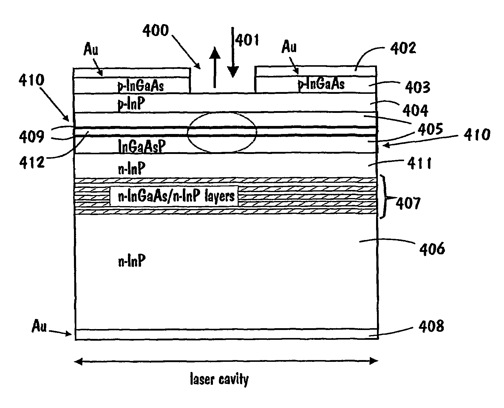
[0023]The basic idea of the invention is to integrate a semiconductor waveguide (edge-emitting type) laser diode with a multiple-quantum-well (MQW) saturable absorber to form a new kind of optical modulator. The modulator can be used in a wide variety of systems, such as in ultra-fast and wideband signal transmission and processing technologies.

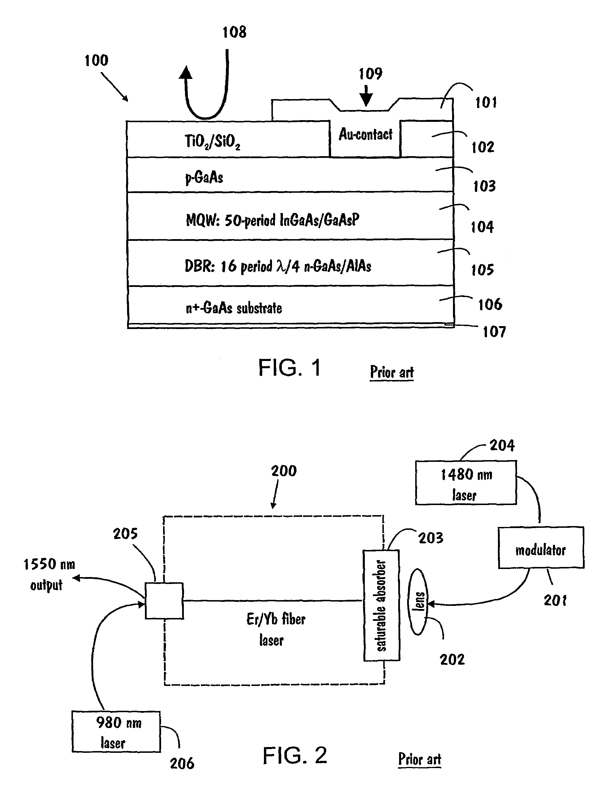
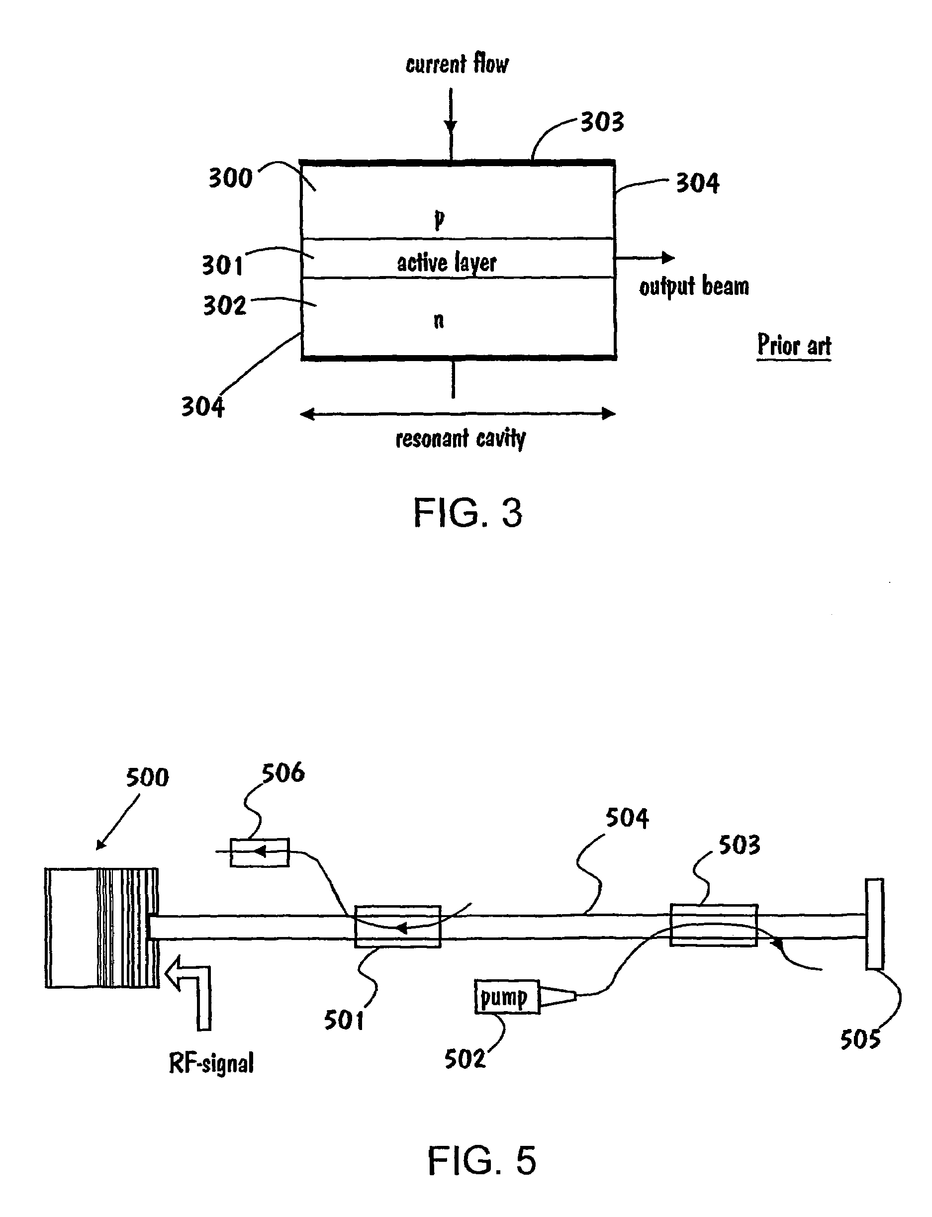
[0024]First we will briefly examine the structure and operation of a laser in general by referring to FIG. 3. Then the structure and operation of the invention is considered in detail with reference to the examples in FIGS. 4a, 4b, and 5.

[0025]FIG. 3 illustrates a cross-sectional view of a semiconductor laser. The laser comprises an active material 301, e.g. MQW, placed between a p-type semiconductor 300, which is doped with suitable impurity atoms and has an excess concentration of holes, and an n-type semiconductor 302 that has an excess concentration of electrons. The refractive index of this lapsing medium or active layer 301 must be grea...


PUM

PropertyMeasurementUnit
wavelengthaaaaaaaaaa
structureaaaaaaaaaa
metallicaaaaaaaaaa

Abstract

The invention relates to an optically pumped multilayered modulator having surface-normal geometry. The multilayer structure comprises an absorber section through which an optical signal (401) to be modulated is coupled from an input (401) to an output (400). The multilayer structure further comprises control means for supplying a control signal for controlling the transmission characteristics of the absorber section. The control signal is generated by an in-plane waveguide-type laser integrated monolithically with the saturable absorption region. The in-plane control laser includes waveguide regions (405) and multiple-quantum-well layers (409) used as a gain medium. The laser beam is adapted to travel through the absorber section in order to modulate the transmission characteristics of the absorber section.

Description

CROSS REFERENCE TO RELATED APPLICATION[0001]This application is a continuation of International Application PCT / FI03 / 00299 filed 16 Apr. 2003 and published in English 6 Nov. 2003 under International Publication Number WO 03 / 091800.FIELD OF THE INVENTION[0002]The present invention relates generally to the structure and operation of an optical modulator.BACKGROUND OF THE INVENTION[0003]There is a growing trend to develop smaller and smaller devices by increasing the number of components fabricated on a single wafer. In the field of high-speed, wide-band optical signal processing and interconnecting technology, a small-sized, low-cost, and efficient modulator is needed. One of the most promising modulators for such applications is a semiconductor surface-normal modulator. It has many advantages, such as low power consumption, small size, polarization insensitivity, simplicity in light coupling, and fiber pigtailing. Surface-normal modulators are especially useful in applications where ...

Claims


Application Information

Patent Timeline
Patent Type & Authority Patents(United States)
IPC IPC(8): G02F1/365H01S5/34G02F1/00G02F1/01G02F1/35H01S3/067H01S3/098H01S3/106H01S5/00H01S5/026H01S5/06
CPCG02F1/3523H01S5/0265H01S3/067H01S3/1061H01S5/0609H01S5/0602H01S3/1118
Inventor OKHOTNIKOV, OLEGGUINA, MIRCEA
Owner NOKIA SOLUTIONS & NETWORKS OY
Why Eureka
Try Eureka