Light-emitting and electron-emitting devices having getter regions

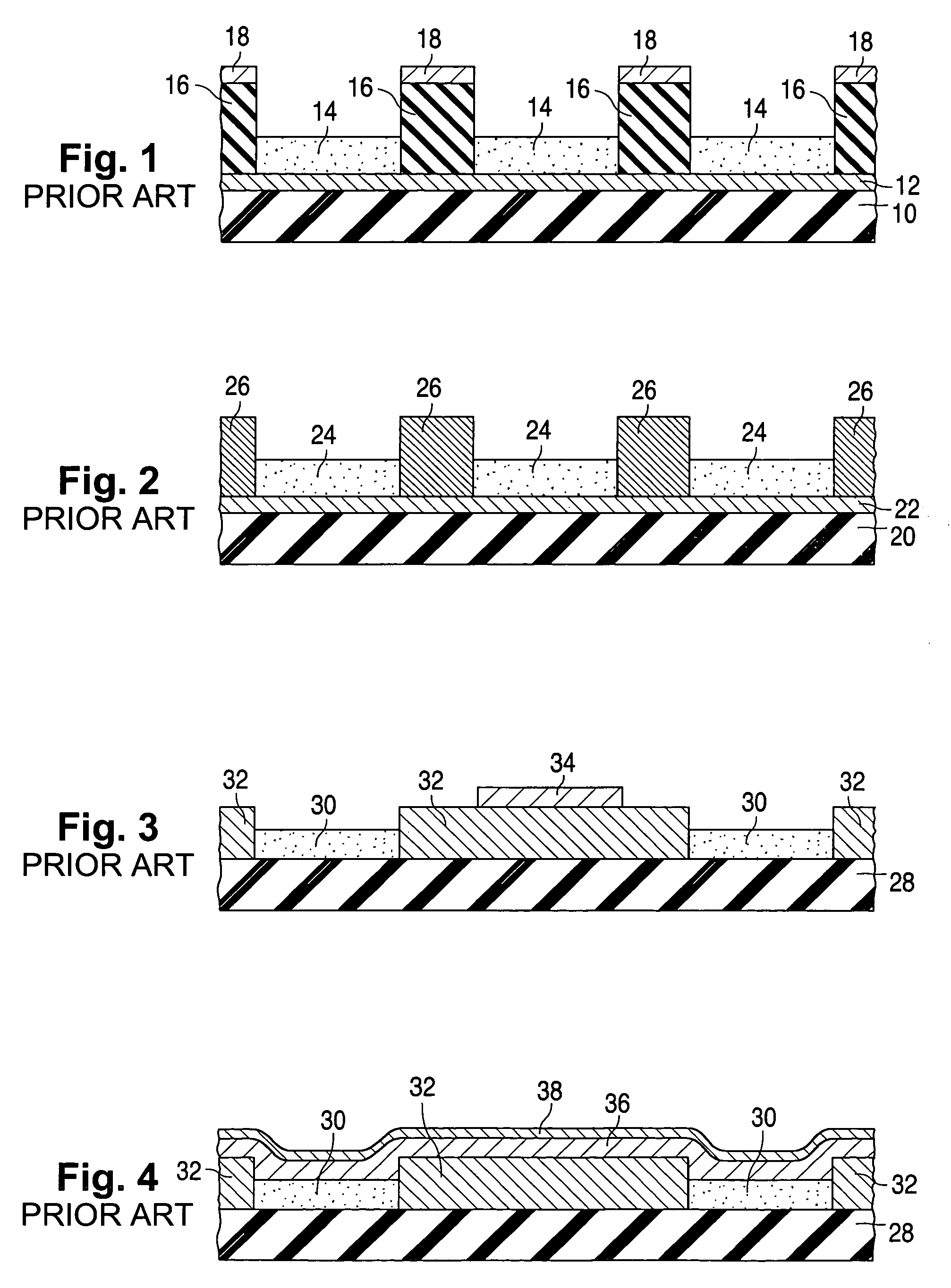
a technology of light-emitting electrons and getters, which is applied in the direction of vacuum obtaining/maintenance, tubes with screens, discharge tubes luminescnet screens, etc., can solve the problems of reducing display life, non-uniform display brightness, and prior art devices of figs. 1–4, etc., to increase the ability of the getter material to provide this assistance, increase the thickness (or height) of the getter material, and enhance the display's performance

Inactive Publication Date: 2008-01-01
CANON KK +1
View PDF68 Cites 29 Cited by
  • Summary
  • Abstract
  • Description
  • Claims
  • Application Information

AI Technical Summary

Benefits of technology

[0039]A relatively thick layer of getter material can normally be deposited by thermal spraying. When the component that receives the thermally sprayed getter material is a light-emitting device situated opposite an electron-emitting device in a flat-panel CRT display, the getter material typically overlies a light-blocking region having an opening in which a light-emissive region is at least partially situated. The light-blocking region typically enhances the display's performance by collecting electrons that scatter backward off the light-emissive region. Since the getter material overlies the light-blocking region, the getter material assists in collecting such backscattered electrons. The ability of the getter material to provide this assistance increases with increasing thickness (or height) of the getter material. Consequently, depositing getter material by thermal spraying facilitates manufacturing a high-performance flat-panel CRT display.
[0040]Electrophoretic or / and dielectrophoretic deposition can be utilized in a maskless manner to deposit getter material over part of a partially fabricated component of a flat-panel display. To implement maskless electrophoretic / dielectrophoretic deposition of getter material, the component normally contains electrically conductive material to which a suitable potential is applied. The conductive material may, for example, form a control electrode or a focus coating. The getter material then accumulates over the conductive material without significantly accumulating elsewhere on the component. Maskless electrophoretic / dielectrophoretic deposition is advantageous because masking steps, often expensive, are avoided.
[0041]In short, a light-emitting or electron-emitting structure configured according to the invention contains a getter region situated in an active portion of the structure so as to achieve a high getter area without significantly increasing the structure's overall lateral area. The lifetime of the light-emitting or electron-emitting structure is significantly increased when it is used in a high-vacuum environment. The light-emitting structure of the invention avoids the transmission losses and other disadvantages of the prior art light-emitting devices mentioned above. The getter material can be deposited by a technique which readily enables the getter material to accumulate where it is needed without contaminating, or otherwise harming, other parts of the light-emitting or electron-emitting structure. The present invention thereby provides a large advance over the prior art.

Problems solved by technology

Contaminant gases in the enclosure can degrade the display and cause various problems such as reduced display lifetime and non-uniform display brightness.
However, the prior art devices of FIGS. 1–4 all have significant disadvantages.
Although the FED of U.S. Pat. No. 5,866,978 avoids many of the disadvantages of the FEDs of FIGS. 1–4, placing getter material only along the outer wall may not yield sufficient getter surface area to achieve long display life.
However, the density of separate electron-emissive sites is relatively low in the display of EPP 996,141 and can lead to non-uniformities in the display's image intensity.

Method used


Image

  • Light-emitting and electron-emitting devices having getter regions
  • Light-emitting and electron-emitting devices having getter regions
  • Light-emitting and electron-emitting devices having getter regions

Examples


Embodiment Construction

General Considerations

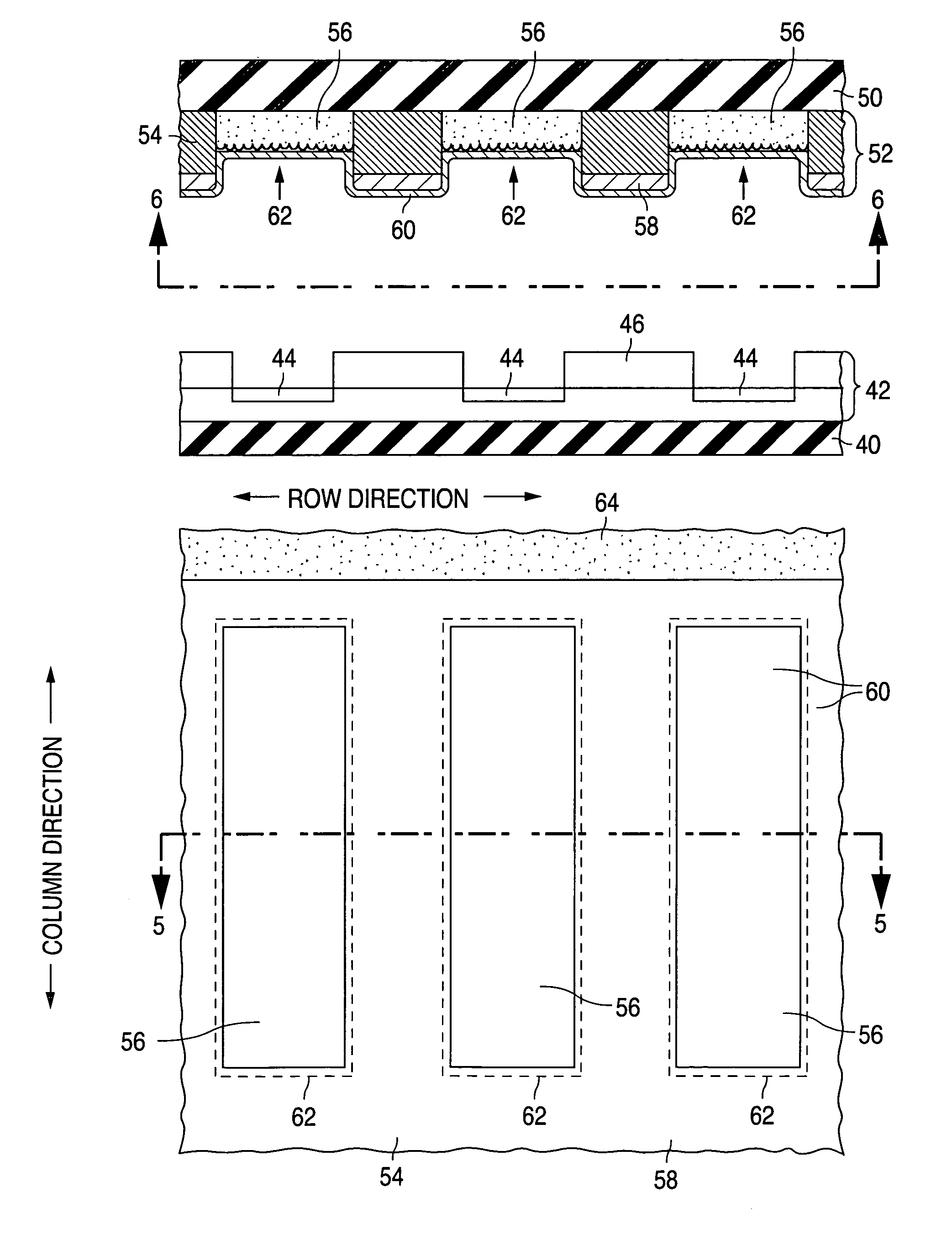
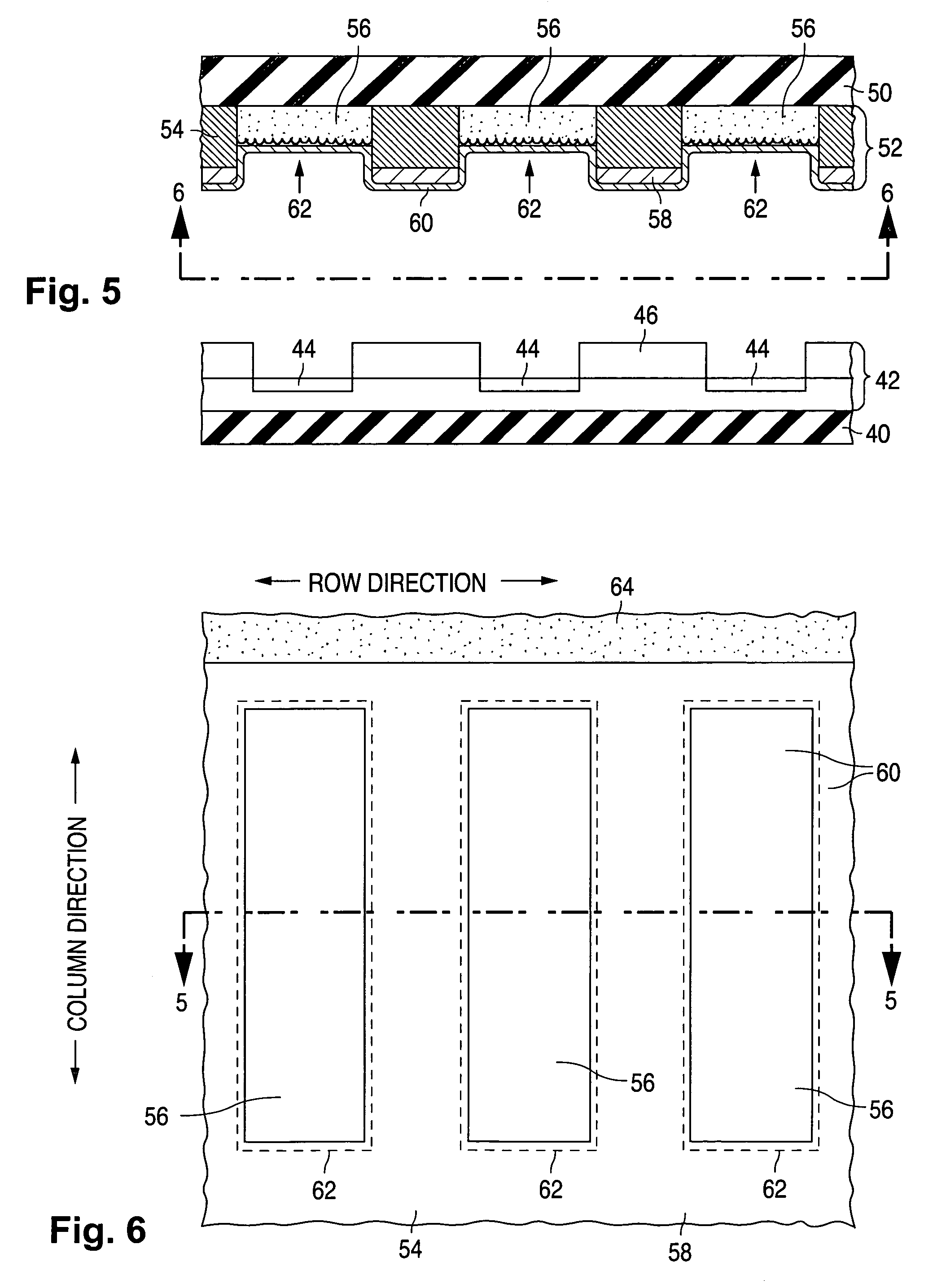
[0075]Various configurations are described below for light-emitting and electron-emitting devices provided with getter regions in accordance with the invention. Each of the electron-emitting devices operates according to field-emission principles and is often referred to here as a field emitter. When one of light-emitting devices is combined with one of the field emitters, the combination forms a field-emission display (again, “FED”).

[0076]Each of the present light-emitting devices can generally be combined with an electron-emitting device other than one of those described below. For example, each of the present electron-emitting devices can be combined with an electron-emitting device which operates according to thermal emission or another technique besides field emission. In that event, the combination of the light-emitting and electron-emitting devices is simply a flat-panel CRT display. Similarly, each of the present electron-emitting devices can be combine...


PUM

PropertyMeasurementUnit
electric fieldaaaaaaaaaa
internal pressureaaaaaaaaaa
temperatureaaaaaaaaaa

Abstract

A light-emitting device contains getter material (58) typically distributed in a relatively uniform manner across the device's active light-emitting portion. An electron-emitting device similarly contains getter material (112, 110/112, 128, 132, and 142) typically distributed relatively uniformly across the active electron-emitting portion of the device.

Description

FIELD OF USE[0001]This invention relates to devices having getters for sorbing (adsorbing or / and absorbing) contaminant gases. More particularly, this invention relates to the structure and fabrication of getter-containing light-emitting devices and electron-emitting devices suitable for use as components of flat-panel cathode-ray tube (“CRT”) displays.BACKGROUND ART[0002]A flat-panel CRT display basically consists of an electron-emitting device and a light-emitting device. The electron-emitting device contains electron-emissive elements that emit electrons across a relatively wide area. The electrons are directed toward light-emitting regions distributed across a corresponding area in the light-emitting device. Upon being struck by the electrons, the light-emitting regions emit light which produces an image on the viewing surface of the display.[0003]The electron-emitting device contains a plate, commonly referred to as the backplate, over which the electron-emissive elements are s...

Claims


Application Information

Patent Timeline
Patent Type & Authority Patents(United States)
IPC IPC(8): H01J1/62H01J63/04H01JH01J9/24H01J1/00H01J1/30H01J1/72H01J3/02H01J7/18H01J9/00H01J9/02H01J9/20H01J9/39H01J29/08H01J29/46H01J29/48H01J29/87H01J29/94H01J31/12
CPCH01J1/30H01J3/021H01J9/148H01J29/467H01J29/481H01J29/94H01J2209/385
Inventor CURTIN, CHRISTOPHER J.HAVEN, DUANE A.HOPPLE, GEORGE B.PAN, LAWRENCE S.MASLENNIKOV, IGOR L.NYSTROM, MICHAEL J.LIU, JUN GORDONGLUCK, RANDOLPH S.KOSUGI, TOMOODUNPHY, JAMES C.MORRIS, DAVID L.
Owner CANON KK
Why Eureka
Try Eureka