System and method for measuring thin film thickness variations and for compensating for the variations

a thin film thickness and variation technology, applied in the direction of image data processing, decorative surface effects, decorative arts, etc., can solve the problems of large change in reflectivity, small thickness variation of different dies, and interference patterns

Active Publication Date: 2008-01-01
APPL MATERIALS ISRAEL LTD
View PDF6 Cites 34 Cited by
  • Summary
  • Abstract
  • Description
  • Claims
  • Application Information

AI Technical Summary

Problems solved by technology

The interference results from multiple reflections of light between two substrates of a thin layer (or film) of transparent material.
The multiple reflected beams of radiations undergo distinct optical paths and generate interference patterns.
Due to the difficulties of producing a uniform layer across the entire wafer during chip manufacturing process, small thickness changes may exist for different dies.
These thickness variations are insignificant for the electrical performance of the IC's but may cause significant reflectivity changes in the course of bright field inspection.
When wafer inspection includes a die-to-die or die-to-database comparison these reflectivity variations may greatly degrade the comparison outcome.
The detected signal can vary substantially as a result of said unknown thickness thus causing detection errors.

Method used


Image

  • System and method for measuring thin film thickness variations and for compensating for the variations
  • System and method for measuring thin film thickness variations and for compensating for the variations
  • System and method for measuring thin film thickness variations and for compensating for the variations

Examples


Embodiment Construction

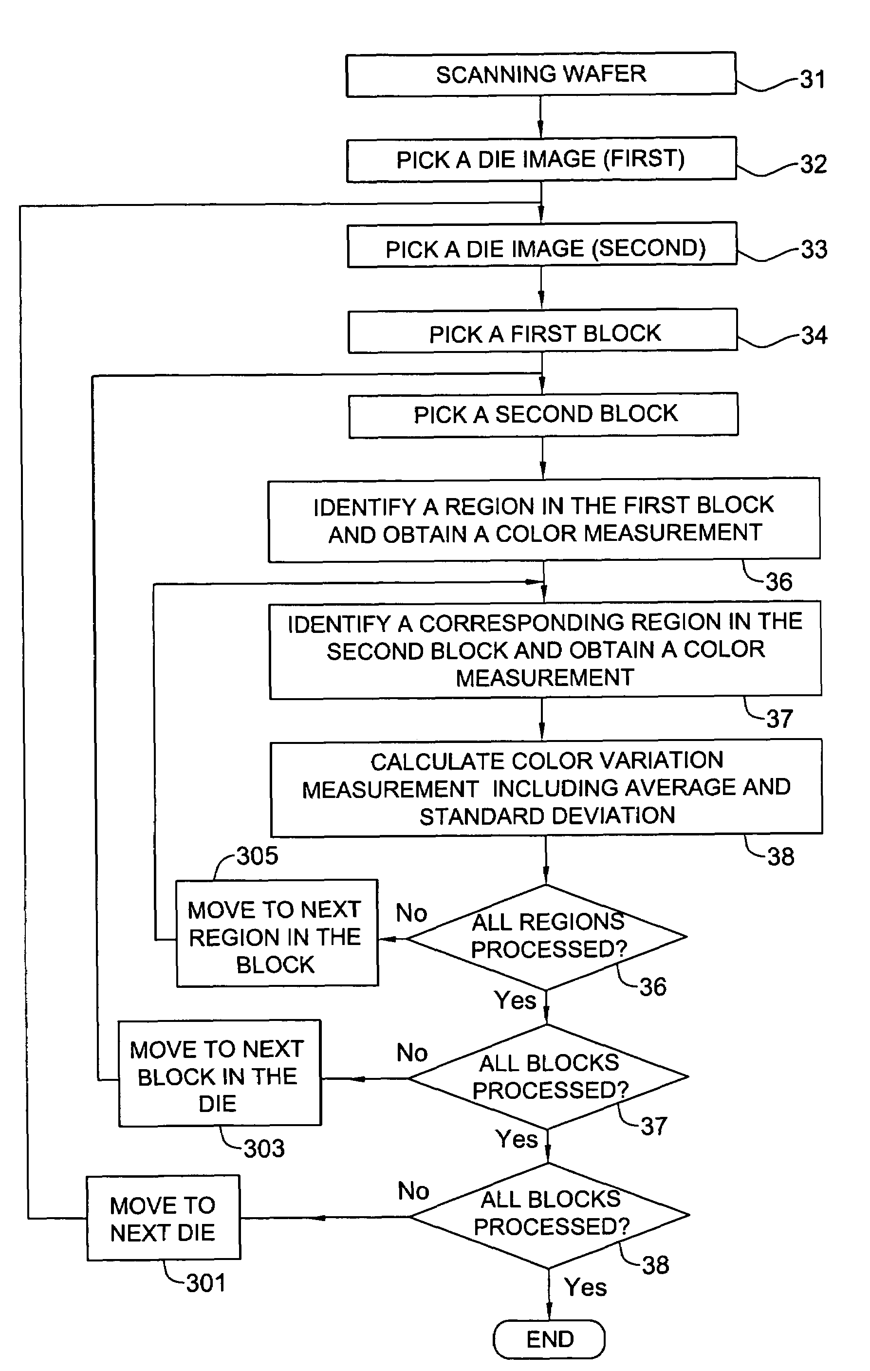
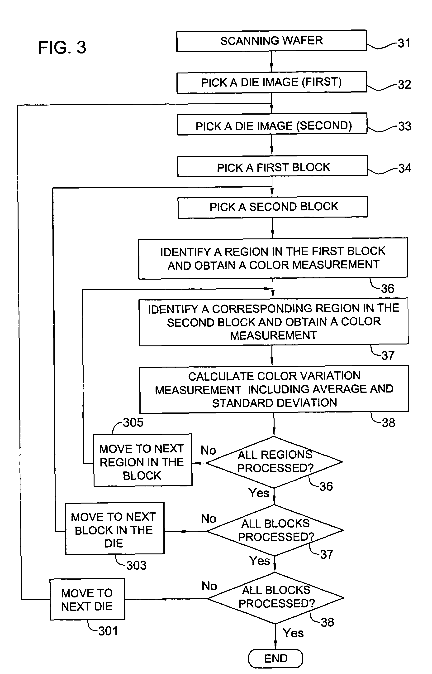
[0050]Those versed in the art will readily appreciate that the various calculation / processing operations described with reference to specific embodiments of the invention are carried out by a processor. Note that the term processor embraces any processing system including one or more processing devices operating in accordance with the following non limiting variants: serially / parallel / distributed and / or in a single location or remote one with respect to the other and communicating through communication network / link. Other variants are applicable, all as required and appropriate.

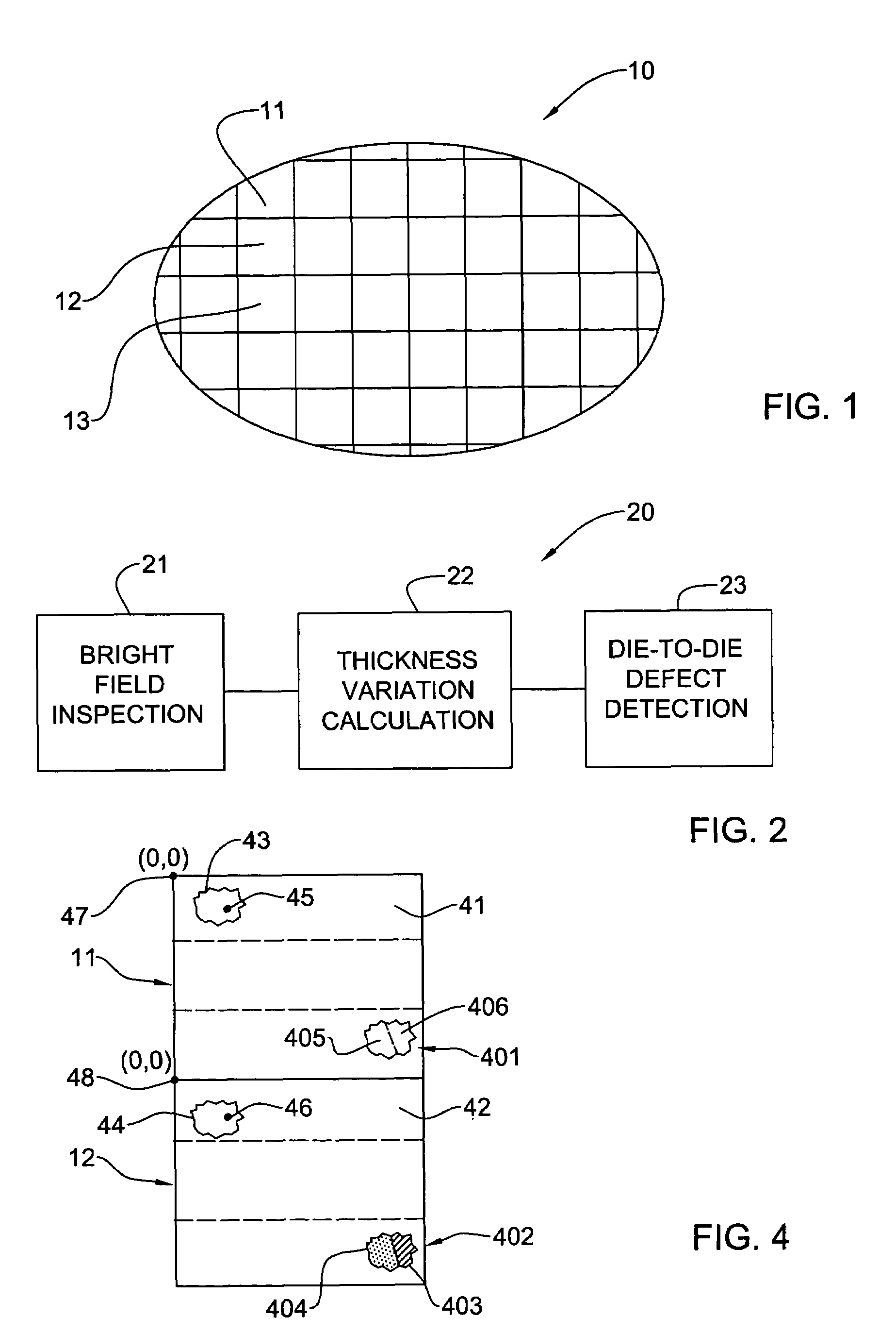
[0051]Note also that thickness variations, such as those introduced by Chemical Mechanical Planarization (CMP) technique are mapped to detected signal Gray Level (GL) variations between ideally identical pixels.

[0052]GL variations (referred to also as detected signal variation) that arise from thickness variations across the wafer are a slow phenomenon compared to pixel changes resulting from defects. Thus, i...


PUM

PropertyMeasurementUnit
thicknessaaaaaaaaaa
widthaaaaaaaaaa
timeaaaaaaaaaa

Abstract

A method for measuring thin film thickness variations of inspected wafer that includes an upper non-opaque thin film. The method including (i) scanning the wafer and obtain wafer image that includes die images each of which composed of pixels, (ii) identifying regions in a first die image and obtain first intensity measurements of the respective regions, (iii) identifying corresponding regions in a second die image and obtain second intensity measurements of the respective regions, (iv) processing the first intensity measurements and the second intensity measurements to obtain signal variations between the second intensity measurements and the first intensity measurements, whereby each calculated signal variation is indicative of thickness variation between a region in the second die and a corresponding region in the first die.

Description

FIELD OF THE INVENTION[0001]This invention relates to signal variation measurement technique for detecting thin film thickness variations across a wafer or reticle.BACKGROUND OF THE INVENTIONRelated Art[0002]Interference involving multiple reflections is known in the art. This phenomenon is described at “Fundamentals of Optics”, F. A. Jenkins and H. E. White, 4th edition, 1976, pages 286-314. The interference results from multiple reflections of light between two substrates of a thin layer (or film) of transparent material. In other words, a single beam of radiation that is directed towards a thin layer of transparent material that is followed by an object that has a refractive index different from the film causes multiple beams of radiations to be reflected from the thin layer. If the object is transparent or partially transparent the single beam of radiation may result in additional multiple transmitted beam of radiations. The multiple reflected beams of radiations undergo distinc...

Claims


Application Information

Patent Timeline
Patent Type & Authority Patents(United States)
IPC IPC(8): G06K9/00B44C1/22H01L31/0232G01B11/02G01N21/95G06T7/00
CPCG01N21/9501G06T7/0004G06T2207/30148
Inventor BARTOV, AVISHAY
Owner APPL MATERIALS ISRAEL LTD
Why Eureka
Try Eureka