
Multilayer plate and display panel with anisotropic crystal film and conducting protective layer

Inactive Publication Date: 2008-01-08
NITTO DENKO CORP
View PDF24 Cites 11 Cited by
  • Summary
  • Abstract
  • Description
  • Claims
  • Application Information

AI Technical Summary

Benefits of technology

[0028]The technical result of the present invention is an increase in the reliability and a decrease in the thickness of LCDs, as well as in the number of operations involved in the LCD assembling process.

Problems solved by technology

The process is quite rapid, taking from a few seconds to several minutes.
Disadvantages of the iodine-containing polarizers are low moisture resistance and thermal stability, which require using various protective layers.
However, use of the polarizers stained with dichroic dyes also requires applying protective layers.
Cutting such polarizers leads to a considerable (up to 20%) amount of wastes.
Polarizers are glued onto an LCD cell after assembly, which introduces additional, technological operations and increases the cost of final products.
However, this increases the number of layers, the total LCD thickness, and the number of technological operations.
Moreover, application of a dichroic polarizer after the formation of electrode system makes the production scheme less flexible, thus hindering changes in the assortment of products.
Another problem in the production of LCDs is their protection from UV radiation.

Method used


Image

  • Multilayer plate and display panel with anisotropic crystal film and conducting protective layer
  • Multilayer plate and display panel with anisotropic crystal film and conducting protective layer
  • Multilayer plate and display panel with anisotropic crystal film and conducting protective layer

Examples


Embodiment Construction

,

[0027]The present invention is aimed at the creation of a multilayer plate which can be used in the production of liquid crystal displays (LCDs), and in particular of thin transmissive or reflective or transflective LCDs with internal polarizers.

[0028]The technical result of the present invention is an increase in the reliability and a decrease in the thickness of LCDs, as well as in the number of operations involved in the LCD assembling process.

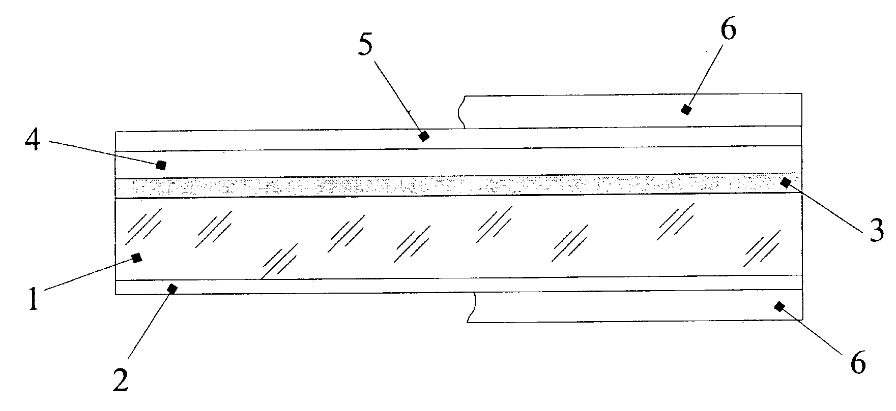
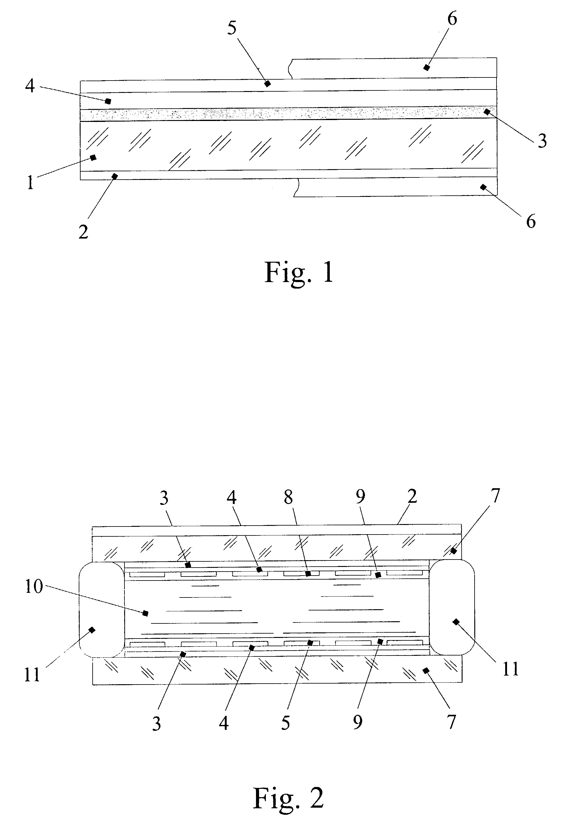
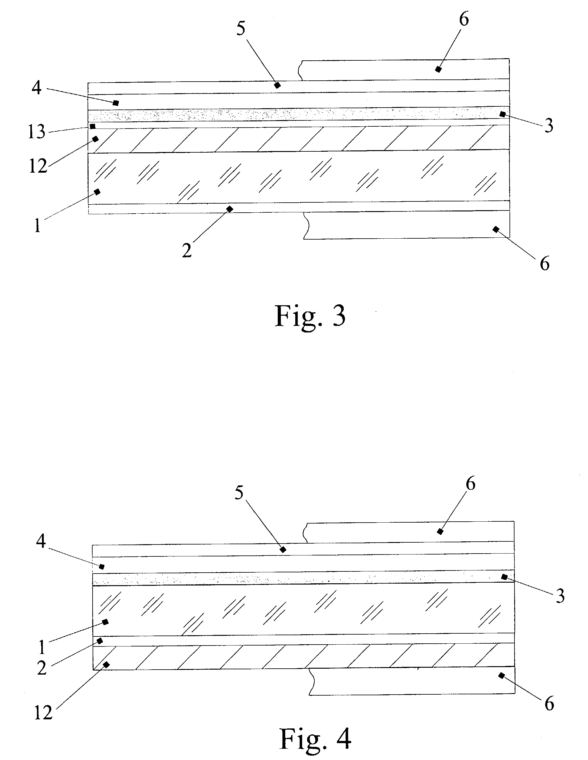
[0029]This technical result is achieved by using a multilayer plate containing a substrate, a protective layer, a conducting layer, and at least one layer of an anisotropic thin crystal film. The thin crystal film represents a substance containing aromatic rings and possesses an interplanar spacing (Bragg's reflection) of 3.4±0.2 Å along one of the optical axes. At least one layer of the thin crystal film is confined between the substrate and the conducting layer, and separated from the conducting layer by a special protective layer. The t...


PUM

PropertyMeasurementUnit
Fractionaaaaaaaaaa
Fractionaaaaaaaaaa
Fractionaaaaaaaaaa

Abstract

A multilayer plate is provided comprising an optically transparent substrate, a protective layer, a conducting layer, and at least one anisotropic thin crystal film. The anisotropic thin crystal film is made of a substance containing aromatic rings and possessing a structure with an interplanar spacing of 3.4±0.2 Å along one of optical axes. The thin crystal film is situated between the substrate and the conducting layer and is separated from the conducting layer by the protective layer. The transmission of the multilayer plate for UV radiation does not exceed 1% at any wavelength below 380 nm.

Description

RELATED APPLICATION[0001]This application claims priority to the U.S. Provisional Patent Application No. 60 / 405,581 filed Aug. 22, 2002, the entire disclosure of which is hereby incorporated by reference.FIELD OF THE INVENTION[0002]This invention relates generally to devices for data display, and in particular to elements of liquid crystal display panels.BACKGROUND OF THE INVENTION[0003]Traditionally, a liquid crystal display (LCD) represents a flat cell comprising two plane-parallel base plates and a system of electrodes. The electrodes are made of an optically transparent, conducting material, for example, a solid solution of indium and tin oxides (ITO), In2O3 and SnO2, and formed on the inner surfaces of the plates. The surface of the plate with electrodes is usually coated with a layer of polyimide or some other polymer and subject to a special treatment ensuring required homogeneous alignment of the molecules of a liquid crystal at the surface and in the bulk of a liquid crysta...

Claims


Application Information

Patent Timeline
IPC IPC(8): G02F1/1335G02B5/30B32B7/02B32B9/00B32B17/00B32B27/00G02F1/1333G02F1/1343
CPCG02F1/133509G02F1/133528Y10T428/10G02F2001/1398Y10T428/1095G02F2001/133565C09K2323/061C09K2323/00G02F1/133565G02F1/1398G02F1/1335
Inventor PAUKSHTO, MICHAEL V.LAZAREV, PAVEL I.
Owner NITTO DENKO CORP
Learn More