Symmetrical clock distribution in multi-stage high speed data conversion circuits

a clock distribution and high-speed data technology, applied in the field of high-speed serial bit stream communication, can solve the problems of high cost and difficulty in manufacturing, low effective yield of indium-phosphate or silicon-germanium process, and difficult to convert data. , to achieve the effect of reducing the skewing of the clock

Inactive Publication Date: 2008-01-15
AVAGO TECH WIRELESS IP SINGAPORE PTE
View PDF6 Cites 1 Cited by
  • Summary
  • Abstract
  • Description
  • Claims
  • Application Information

AI Technical Summary

Benefits of technology

[0011]The present invention provides a high-speed data conversion circuit. More specifically, a high-speed data conversion circuit that simultaneously reduces the skewing of clock, data and other like signals, and as well as power consumption.

Problems solved by technology

Particular difficulties arise in converting data between the 40×1 GBPS line interface and the 16×2.5 GBPS communication ASIC interface.
While other materials, e.g., Indium-Phosphate and Silicon-Germanium provide higher switching rates than do Silicon based devices, they are very expensive and difficult to manufacture.
Thus, even if a device were manufactured that could perform such interfacing operations, the effective yield in an Indium-Phosphate or Silicon-Germanium process would be very low.
Skewing of data and clock signals in high-speed data communications systems running at clock and data rates in the 10 GBPS range can be very difficult to avoid and can adversely impact the integrity of data.
Some prior art solutions involved delay schemes that consume power and increase the overall complexity of these circuits.

Method used


Image

  • Symmetrical clock distribution in multi-stage high speed data conversion circuits
  • Symmetrical clock distribution in multi-stage high speed data conversion circuits
  • Symmetrical clock distribution in multi-stage high speed data conversion circuits

Examples


Embodiment Construction

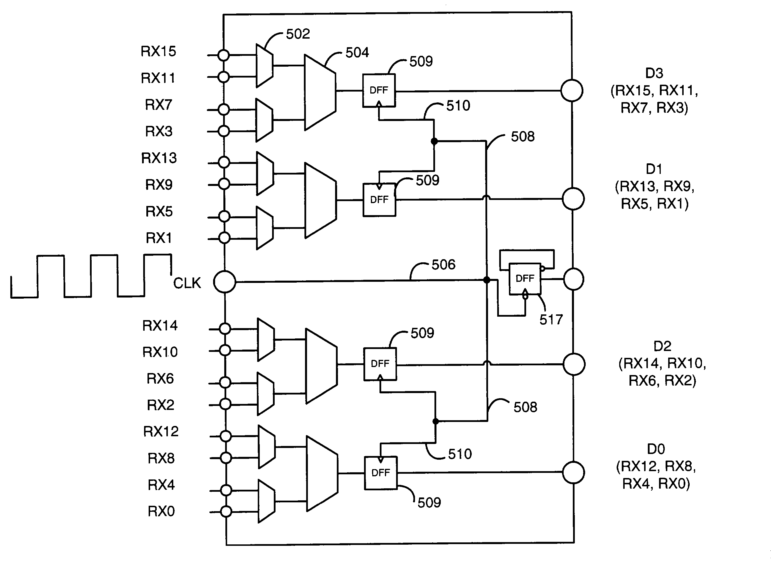
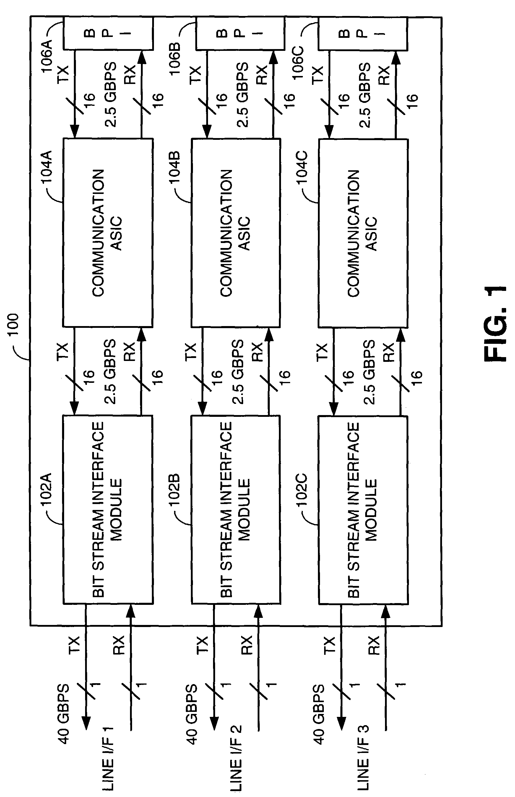
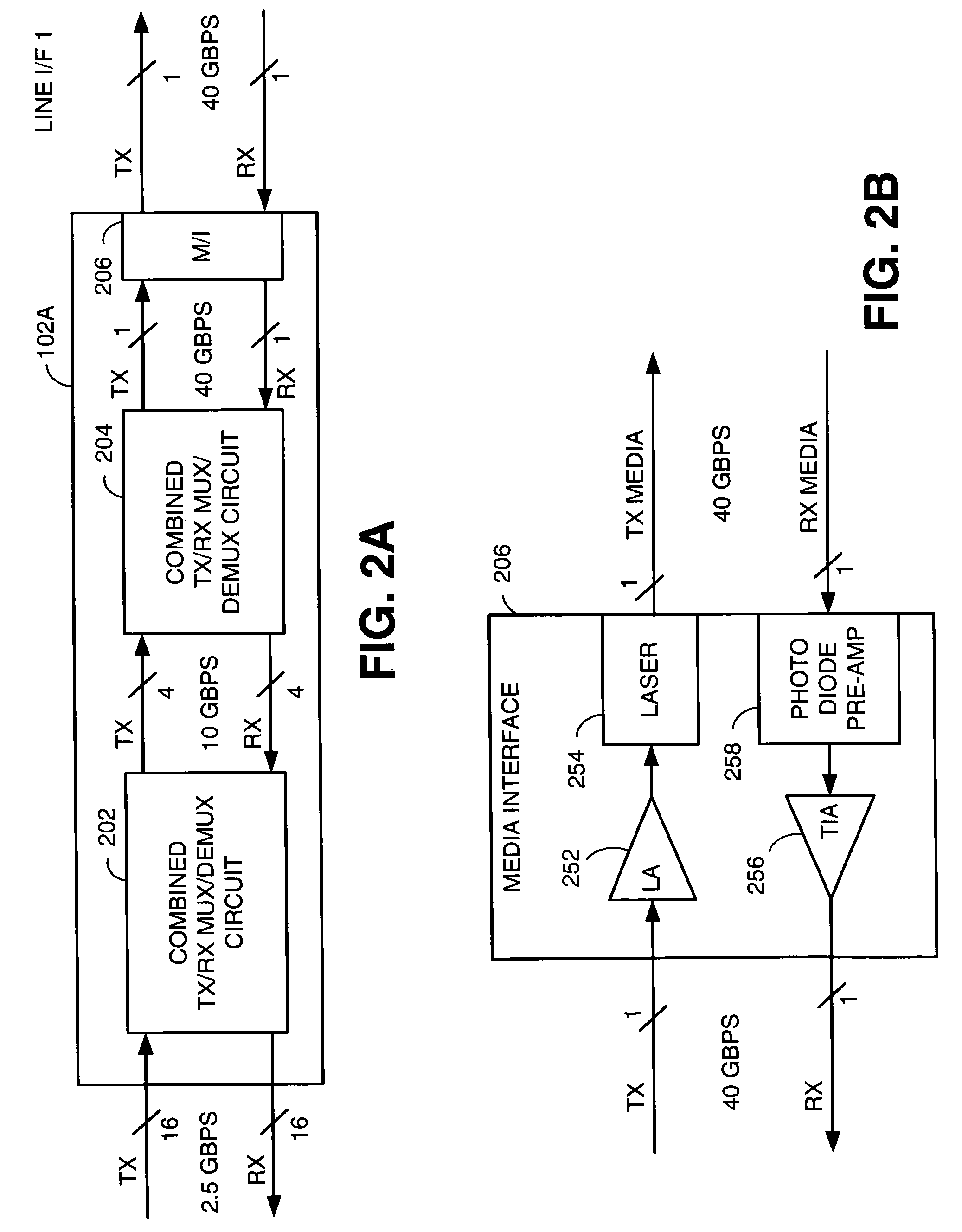
[0040]FIG. 1 is a block diagram illustrating a Printed Circuit Board (PCB) that has mounted thereon a plurality of Bit Stream Interface Module (BSIMs) constructed according to the present invention. As shown in FIG. 1, the PCB 100 includes BSIMs 102A, 102B and 102C. The PCB 100 also includes mounted thereupon communication Application Specific Integrated Circuits (ASIC) 104A, 104B, and 104C. The PCB 100 is mounted within a housing that services switching requirements within a particular location or geographic area. Each of the BSIMs 102A, 102B, and 102C couples to a high-speed media such as an optical fiber via a respective media interface and supports the OC-768 or the SEC-768 standard at such media interface. On the second side of the BSIMs 102A through 102C, the SFI-5 interface standard is supported. Communication ASIC 104A through 104C may communicate with other PCB components located in the housing via back interfaces 106A through 106C.

[0041]The BSIMs 102A through 102C may be r...


PUM


Abstract

The present invention provides a high speed bit stream data conversion circuit that includes input ports to receive first bit streams at a first bit rate. Data conversion circuits receive the first bit streams and produce second bit stream(s), wherein the number and bit rate of the first and second bit stream(s) differ. Symmetrical pathways transport the first bit streams from the input ports to the data conversion circuits, wherein their transmission time(s) are substantially equal. A clock distribution circuit receives and symmetrically distributes a clock signal to data conversion circuits. A central trunk coupled to the clock port and located between a first pair of circuit pathways with paired branches that extend from the trunk and that couple to the data conversion circuits make up the clock distribution circuit. The distributed data clock signal latches data in data conversion circuits from the first to the second bit stream(s).

Description

RELATED APPLICATION[0001]This application claims priority to U.S. Provisional Application Ser. No. 60 / 403,457, filed Aug. 12, 2002, and to U.S. Regular Utility application Ser. No. 10 / 445,771 filed May 27, 2003, both of which are incorporated herein by reference in their entirety for all purposes.TECHNICAL FIELD OF THE INVENTION[0002]The present invention relates generally to communication systems; and more particularly to high-speed serial bit stream communications.DESCRIPTION OF RELATED ART[0003]The structure and operation of communication systems is generally well known. Communication systems support the transfer of information from one location to another location. Early examples of communication systems included the telegraph and the public switch telephone network (PSTN). When initially constructed, the PSTN was a circuit switched network that supported only analog voice communications. As the PSTN advanced in its structure and operation, it supported digital communications. T...

Claims


Application Information

Patent Timeline
Patent Type & Authority Patents(United States)
IPC IPC(8): H04J3/02H04J3/04H04J3/06H04L7/00
CPCH04J3/04H04J3/0685H04J3/0629H04L7/0008
Inventor YIN, GUANGMINGZHANG, BONEJAD, MOHAMMADCAO, JUN
Owner AVAGO TECH WIRELESS IP SINGAPORE PTE
Why Eureka
Try Eureka