Method and apparatus for optically measuring the topography of nearly planar periodic structures

a technology of optical measurement and periodic structure, applied in the direction of amplifiers, transmission, complex mathematical operations, etc., can solve the problems of distorted images, inability to measure high aspect ratio, and alter the structure to be measured

Inactive Publication Date: 2008-01-22
DANSK FUNDAMENTAL METROLOGI
View PDF16 Cites 11 Cited by
  • Summary
  • Abstract
  • Description
  • Claims
  • Application Information

AI Technical Summary

Problems solved by technology

However, electron beam imaging has some drawbacks:1. The method does not reveal depth information2. Destructive method when profile of the structure is measured by cross-sectional technique3. Sample environment during measurement is vacuum4. Conductive coating of non-conductive structures is necessary in order to enhance the generation of secondary electrons.
This alters the structure to be measured.5. Build-up of surface charge affects the measurement resulting in distorted images
The technique gives features of few nanometers, however the technique suffers from1. Topographical distortions of image due to folding of probe shape and surface.2. Structures having high aspect ratio cannot be measured.
Both the electron beam imaging and the scanning probe microscopy suffer from being operator demanding and time consuming.
Another limitation to these techniques is lack of measuring embedded structures in samples.
However, resolution of lateral features is limited by the spot size of the light beam, which is in the range of a micron.
However, the apparatus and method of U.S. Pat. No. 5,963,329 has the following disadvantages:1. It may only be applied to symmetric periodic line structures,2. the recorded data used in the profile determination is only sufficient for symmetric structures.
The method disclosed in U.S. Pat. No. 6,281,974 suffers from basically the same drawbacks as U.S. Pat. No. 5,963,329—namely, that since only information in the zero order diffraction beam is recorded the profile determination is only sufficient for symmetric structures.
An attempt to apply the method of U.S. Pat. No. 6,281,974 to asymmetric profiles will lead to un-determined equation systems that are incapable of calculating the profile in an unambiguous manner.

Method used


Image

  • Method and apparatus for optically measuring the topography of nearly planar periodic structures
  • Method and apparatus for optically measuring the topography of nearly planar periodic structures
  • Method and apparatus for optically measuring the topography of nearly planar periodic structures

Examples


Embodiment Construction

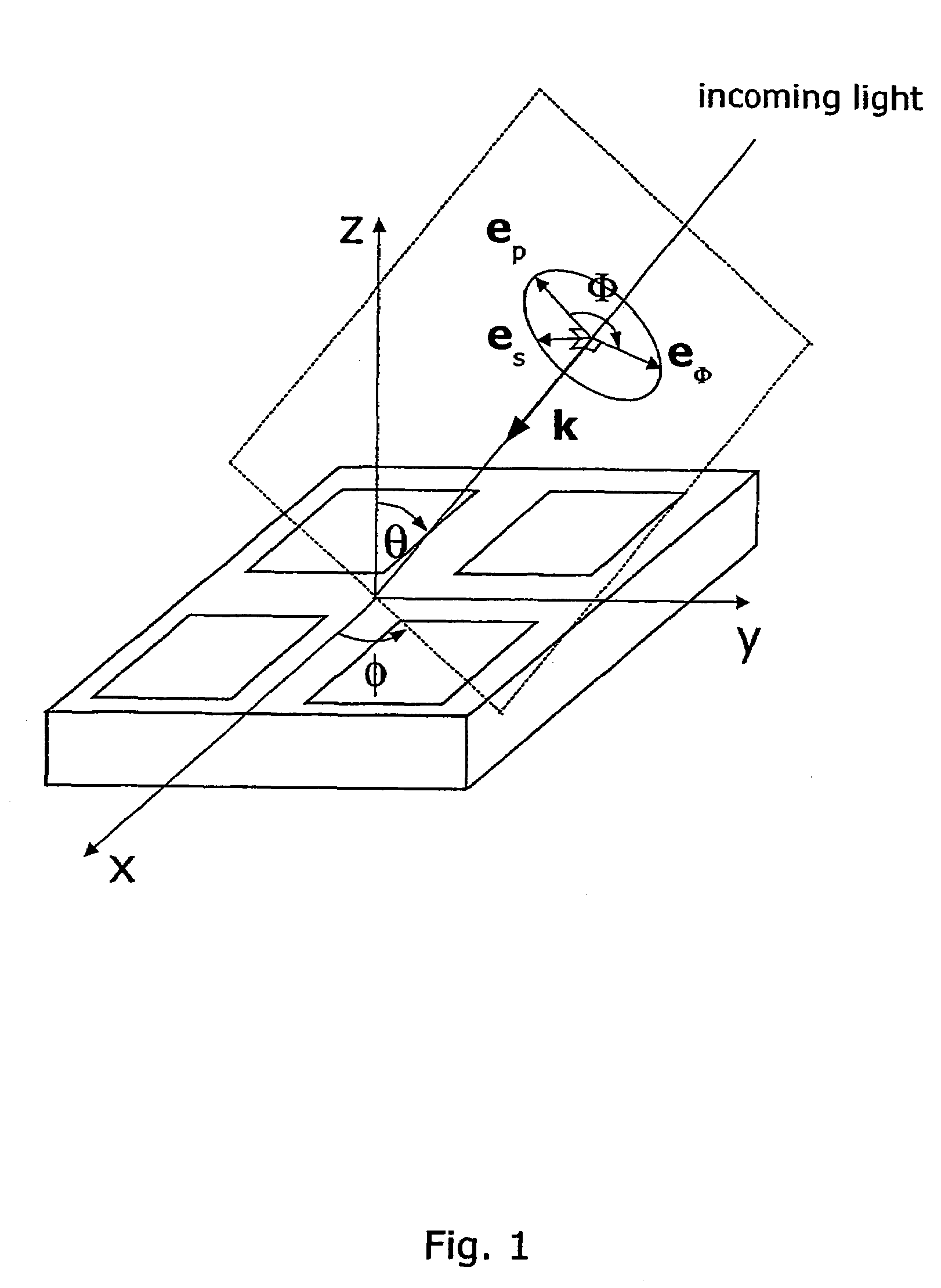
[0098]An illustration of the principle of the invention is in FIGS. 1-9. In FIG. 1 is defined the illumination geometry of a sample having a locally repeated structure. The structure is Illuminated by a plane electromagnetic wave characterized by its wavelength λ, linear polarization Φ, and the direction of propagation given by the incident angle θ and the azimuth angle φ. The Cartesian coordinate system has the x-axis along one of the periodic directions.

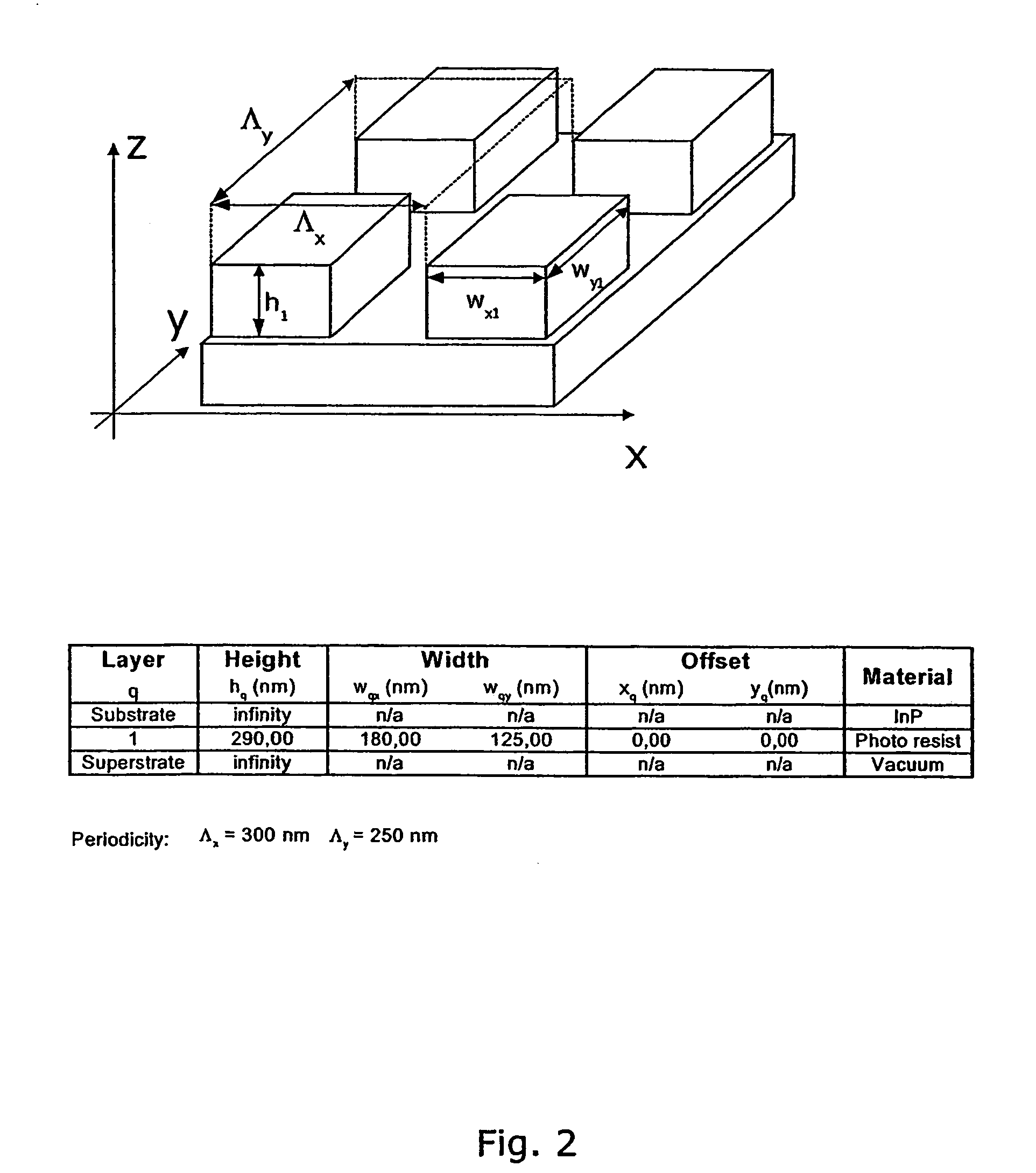
[0099]The intensity of light diffracted by the structure normalized to the intensity of the incident light, denoted as the diffraction efficiency, is calculated for a symmetric profile represented by a box in FIG. 2 and an asymmetric profile described in FIG. 3. The latter profile alters just slightly from the rectangular profile. In FIGS. 4-6 are plotted the calculated diffraction efficiency as function of wavelength for various diffraction orders, and in FIG. 7-9 are plotted the calculated diffraction efficiency as function of in...


PUM


Abstract

The present invention discloses a non-destructive method and apparatus for measuring the 3D topography of a sample having periodic microstructure deposited onto the surface, or deposited onto a film, or buried into the film or sample. In particular, the present invention relates to an optical system and method utilizing polarized light beam, diffracted from the repeated structure, to measure its spatial geometry giving parameters such as profile height, profile widths, sidewall angles, and arbitrary profile shape. The optical system employs a broadband or semi-monochromatic light source to produce a light beam that is polarized and focused onto the periodic structure being measured. The focused beam consists of a whole range of illumination angles that is provided to the structure simultaneously. Transmitted or reflected diffracted light generated by the interaction of the light with the periodic structure is collected by an imaging detector system. The detector records the diffraction light irradiance resolved into illumination angles, diffraction orders and wavelength. The data is applied to determine the geometrical profile of the periodic structure using a reconstruction algorithm that is based on comparisons between measured diffraction data and modeled diffraction irradiance of a profile model using Maxwell's equations. The reconstruction of the profile is performed by iterative adjustments of a profile seed model until the modeled diffraction irradiance matches the measured data within a predefined convergence tolerance.

Description

FIELD OF THE INVENTION[0001]The present invention relates to a method and apparatus for optically measuring the topography of locally periodic microstructures on a nearly planar surface or embedded into nearly planar stratified structures. In particular, the present invention relates to an optical device utilizing light diffracted from semi-periodic microstructure to determine the topography of the structure.BACKGROUND OF THE INVENTION[0002]Process and quality control of semi-periodic microstructures with structures ranging from microns to nanometers plays an important role in fabrication of optoelectronics, optical and microelectronic devices. One approach to perform quality control on a microstructure is to detect the diffracted light intensities from the microstructure. The light intensities for the different diffracted orders together with a computer algorithm may then be used to produce a topographic image of the microstructure.[0003]Process and quality control of microstructur...

Claims


Application Information

Patent Timeline
Patent Type & Authority Patents(United States)
IPC IPC(8): G01B11/14G01B11/06G01B11/24G01B11/30
CPCG01B11/0641G01B11/24G01B11/30
Inventor LARSEN, NIELS AGERSNAPHANSEN, POUL-ERIK
Owner DANSK FUNDAMENTAL METROLOGI
Why Eureka
Try Eureka