

Semiconductor device and manufacturing method thereof
a technology of semiconductors and semiconductors, applied in the direction of semiconductor devices, basic electric elements, electrical equipment, etc., can solve problems such as the level of semiconductors, and achieve the effect of low power consumption design
- Summary
- Abstract
- Description
- Claims
- Application Information
AI Technical Summary
Benefits of technology
Problems solved by technology
Method used
Image

Examples
first embodiment
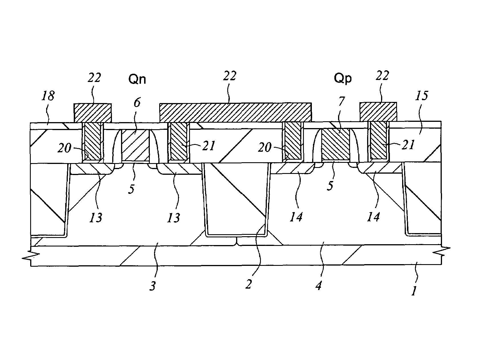
[0071]FIG. 1 is a cross-sectional view showing a semiconductor substrate (hereinafter, referred to as substrate) 1 on which an n channel MIS transistor (Qn) and a p channel MIS transistor (Qp) according to this embodiment are formed.
[0072]A p type well 3 and an n type well 4 whose areas are defined by device isolation trenches 2 are formed on the main surface of the substrate 1 made of p type single crystal silicon. The n channel MIS transistor (Qn) is formed on the p type well 3, and the p channel MIS transistor (Qp) is formed on the n type well 4.
[0073]The n channel MIS transistor (Qn) is provided with a gate insulator 5 formed on the surface of the p type well 3, a gate electrode 6 formed on the gate insulator 5 and n+ type semiconductor regions (source, drain) 13 formed in the p type well 3. Also, the p channel MIS transistor (Qp) is provided with a gate insulator 5 formed on the surface of the n type well 4, a gate electrode 7 formed on the gate insulator 5 and p+ type semicond...
second embodiment
[0100]The manufacturing method of an n channel MIS transistor (Qn) and a p channel MIS transistor (Qp) according to this embodiment will be described with reference to FIG. 15 to FIG. 19.
[0101]First, as shown in FIG. 15, after forming the silicon gate electrode 8 on each of the gate insulators 5 of the p type well 3 and the n type well 4, the n+ type semiconductor regions (source, drain) 13 are formed in the p type well 3 and the p+ type semiconductor regions (source, drain) 14 are formed in the n type well 4. Thereafter, the surface of the silicon oxide film 15 deposited on the substrate 1 is polished and planarized, thereby exposing the surfaces of the silicon gate electrodes 8 on the surface of the silicon oxide film 15. The process so far is identical to that described in the first embodiment shown in FIG. 1 to FIG. 7.
[0102]Next, as shown in FIG. 16, after depositing a silicon nitride film 17 on the substrate 1 by the CVD, the silicon nitride film 17 above the n type well 4 is s...
third embodiment
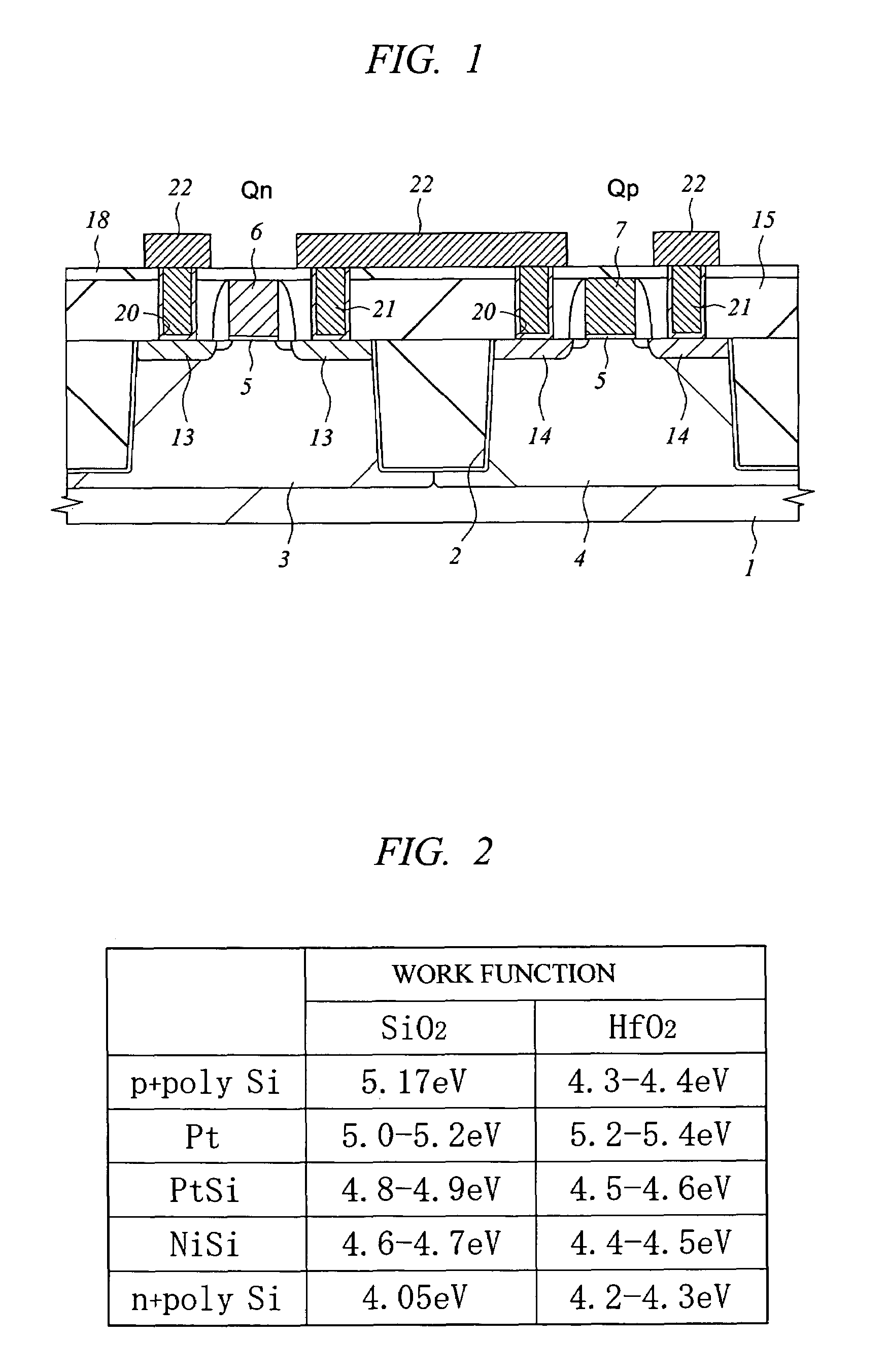
[0112]In the n channel MIS transistor (Qn) according to this embodiment, the gate electrode on the gate insulator composed of a hafnium-based insulator is composed of an n type polycrystalline silicon film doped with phosphorus or arsenic or a metal silicide film made of, for example, Ni silicide. Also, in the p channel MIS transistor (Qp) according to this embodiment, the gate electrode on the gate insulator composed of a hafnium-based insulator is composed of a metal silicide film made of, for example, Pt silicide.
[0113]When a metal silicide film such as a Pt silicide film is used to constitute the gate electrode of the p channel MIS transistor (Qp), the influence of the depletion can be reduced in comparison to the case where a p type polycrystalline silicon film is used to constitute the gate electrode. Consequently, the driving force of the p channel MIS transistor (Qp) whose ON current is basically lower than that of the n channel MIS transistor (Qn) can be improved.
[0114]In a...
PUM
 Abstract
Description
Claims
Application Information