

Method of manufacturing a wiring board
a manufacturing method and wire technology, applied in the field of wire boards, can solve the problems of high material and manufacturing costs, high cost of screen printing a solder paste on a board, and limited pitch reduction between bumps, so as to achieve the effect of perfectly preventing the surface oxidation of the first terminal area
- Summary
- Abstract
- Description
- Claims
- Application Information
AI Technical Summary
Benefits of technology
Problems solved by technology
Method used
Image

Examples
first embodiment
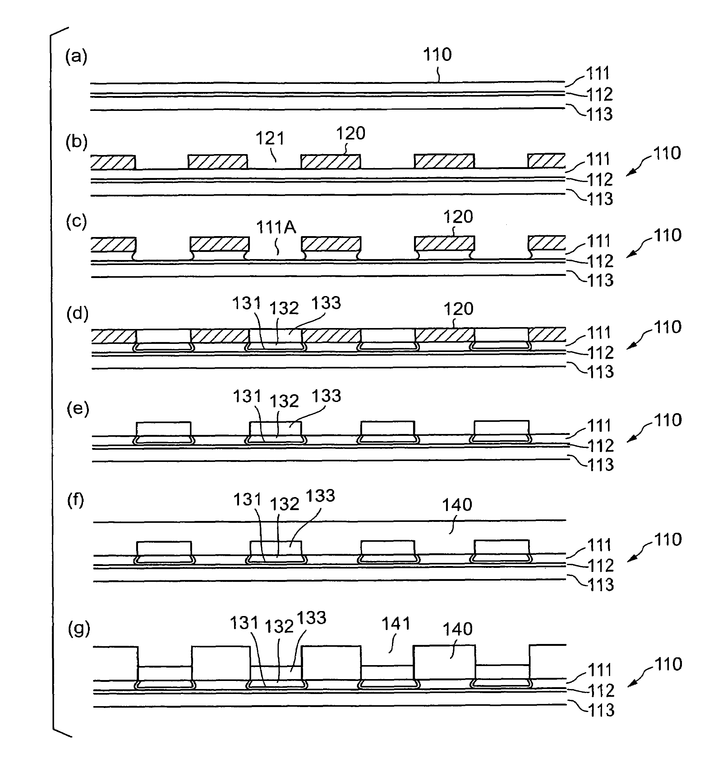
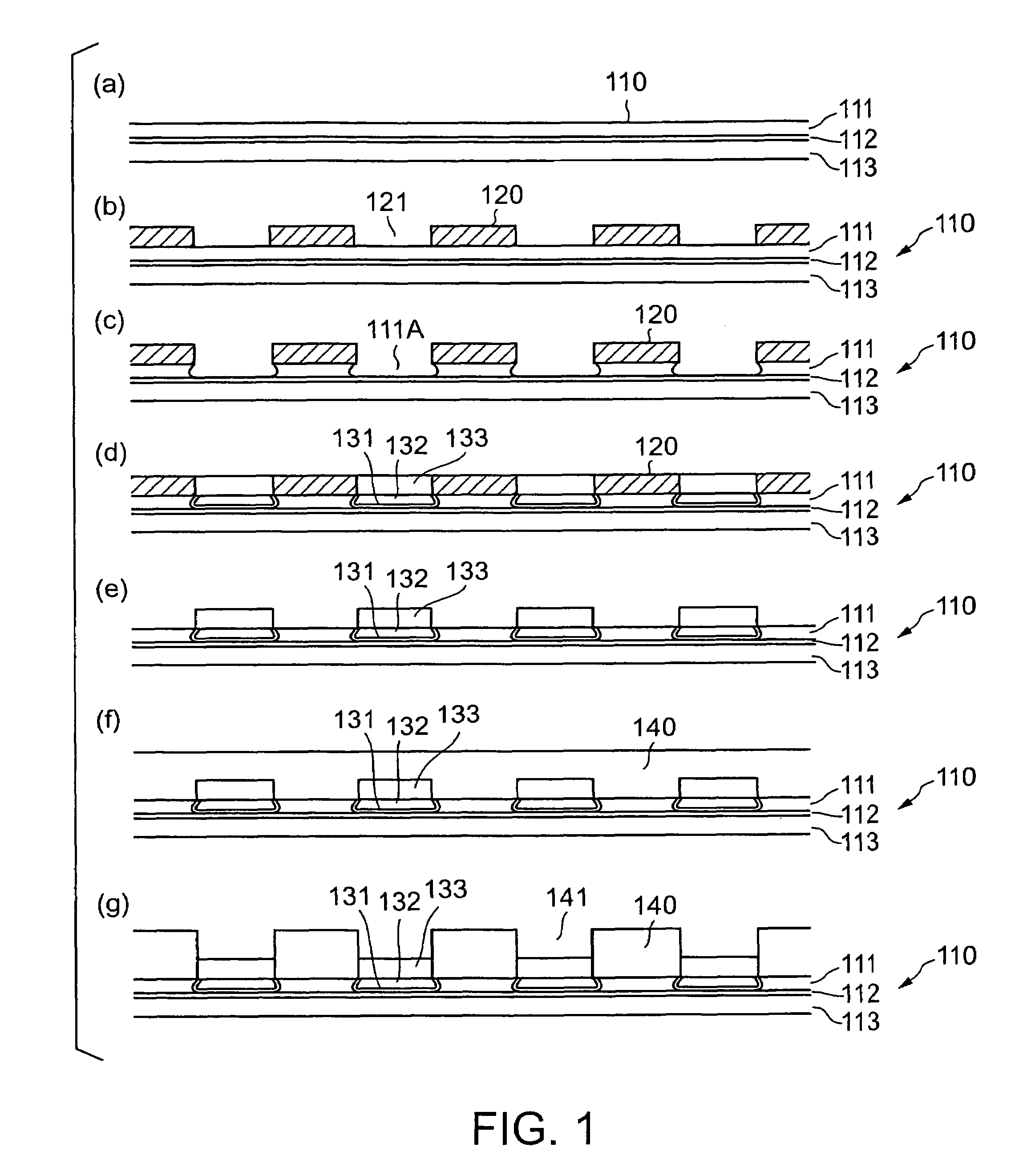
[0063]a method of manufacturing a wiring board according to the present invention is described with reference to FIGS. 1 to 3.
[0064]As shown in FIG. 3(d), a wiring board includes a wiring part formed of two wiring layers 170 and 175, first terminal areas 131, 132, and 133 disposed on one side of the wiring layers 170 and 175 in a projecting manner, and second terminal areas 191 and 192 disposed on the other side of the wiring layers 170 and 175.
[0065]The wiring layers 170 and 175 of the wiring part respectively have resin material layers 140 and 145 on a side where the first terminal areas 131, 132, and 133 are formed. The first terminal areas 131, 132, and 133 constitute a projected bump for flip-chip connection to be directly flip-chip connected to a solder bump of a semiconductor element. The second terminal areas 191 and 192 are formed such that an opening 181 of a solder resist 180 covering the wiring layers 170 and 175 is filled with the second terminal areas 191 and 192.
[0066...
second embodiment
[0095]a method of manufacturing a wiring board according to the present invention is described with reference to FIGS. 4 and 5.
[0096]A wiring board includes a wiring part formed of two wiring layers 270 and 275, first terminal areas 230, 211, 212, and 295 disposed on one side of the wiring layers 270 and 275 in a projecting manner, and second terminal areas 291 and 292 disposed on the other side of the wiring layers 270 and 275 (FIG. 5(d)).
[0097]The wiring layers 270 and 275 of the wiring part respectively have resin material layers 240 and 245 on a side where the first terminal areas 230, 211, 212, and 295 are formed. The first terminal areas 230, 211, 212, and 295 constitute a projected bump for flip-chip connection to be directly flip-chip connected to a solder bump of a semiconductor element. The second terminal areas 291 and 292 are formed such that an opening 281 of a solder resist 280 covering the wiring layers 270 and 275 is filled with the second terminal areas 291 and 292....
PUM
| Property | Measurement | Unit |
|---|---|---|
| thickness | aaaaa | aaaaa |
| thickness | aaaaa | aaaaa |
| thickness | aaaaa | aaaaa |
Abstract
Description
Claims
Application Information