Device, method of manufacturing the same, electro-optic device, and electronic equipment

a manufacturing method and electrooptic technology, applied in the manufacture of electrooptic systems, conductive pattern formation, construction materials, etc., can solve the problems of large scale equipment and complex processes, high manufacturing costs, and only several percent of material usage efficiency, so as to achieve uniform thickness and uneven electric properties.

Inactive Publication Date: 2008-02-05
SEIKO EPSON CORP
View PDF25 Cites 6 Cited by
  • Summary
  • Abstract
  • Description
  • Claims
  • Application Information

AI Technical Summary

Benefits of technology

[0024]Accordingly, in the present invention, although drying of the second conductive film as a dummy wiring makes progress at the ends of the plate where drying proceeds quickly, in the wiring pattern area which is actually used for wiring, the concentration of solvent vapor (atmosphere) becomes uniform due to the presence of the second conductive film, whereby the uniformity of drying and baking atmosphere of the conductive film is achieved, and hence a film of a uniform thickness can be obtained. Therefore, in the present invention, unevenness of electric property, such as conductivity, caused by variations in film thickness can be solved.

Problems solved by technology

The lithography method requires large scale equipment and complex processes such as a vacuum device, and the material usage efficiency is only several percent.
Therefore, most of the material has to be put on the shelf, and hence it requires high manufacturing costs.
However, there are problem as shown below.
However, fine liquid applied on the plate dries very quickly and, in addition, it generally starts drying quickly at the ends (upper end, lower end, right end, and left end) of the applied area on the plate since the partial pressure of the solvent molecules (concentration of solvent vapor) vaporized from the fine liquid at these regions is low.
The difference of drying time of the liquid member applied on the plate as described above causes variations in film thickness of conductive film wiring, and variations in film thickness may cause a defect of unevenness of electric property, such as conductivity.

Method used


Image

  • Device, method of manufacturing the same, electro-optic device, and electronic equipment
  • Device, method of manufacturing the same, electro-optic device, and electronic equipment
  • Device, method of manufacturing the same, electro-optic device, and electronic equipment

Examples


Embodiment Construction

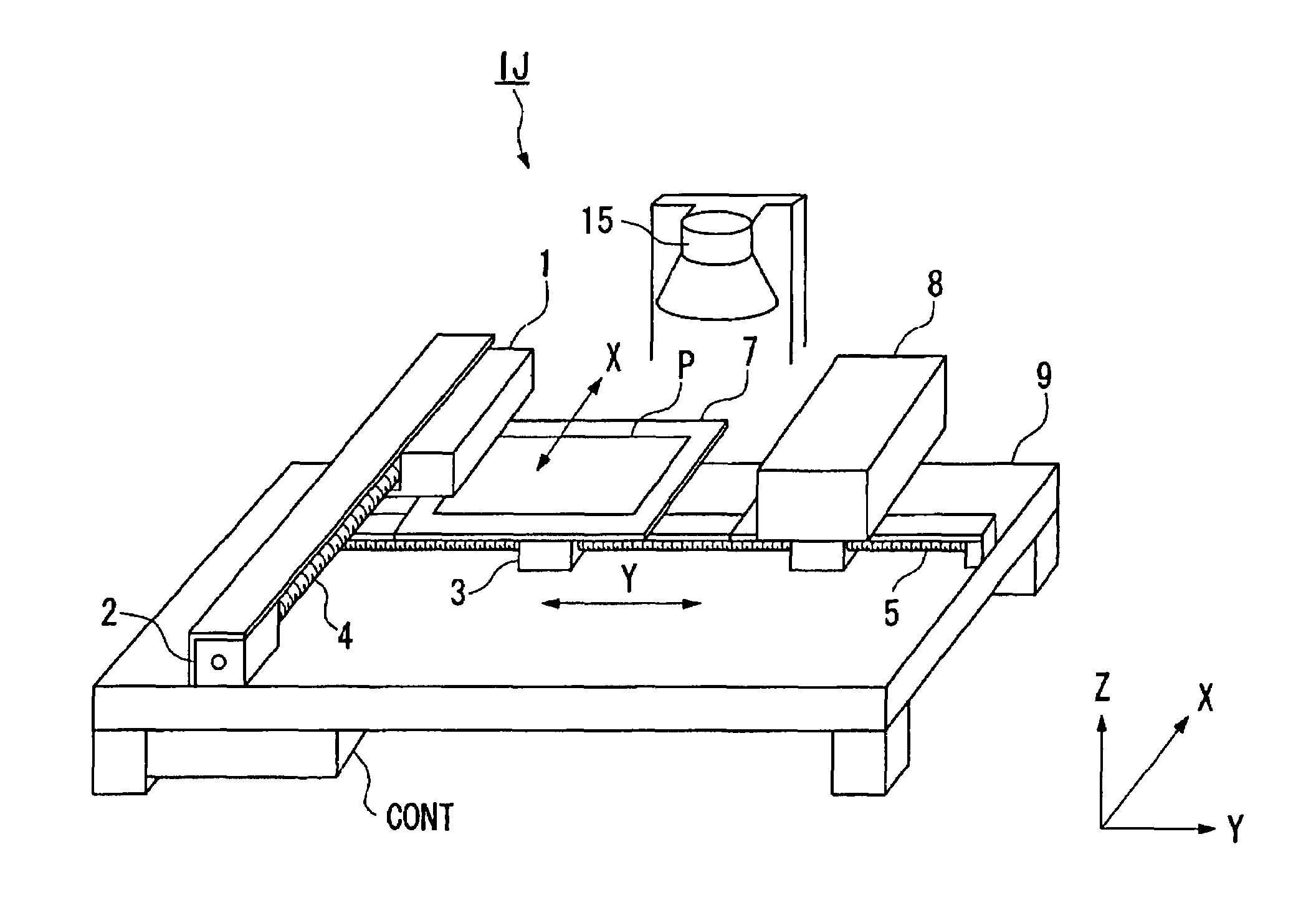
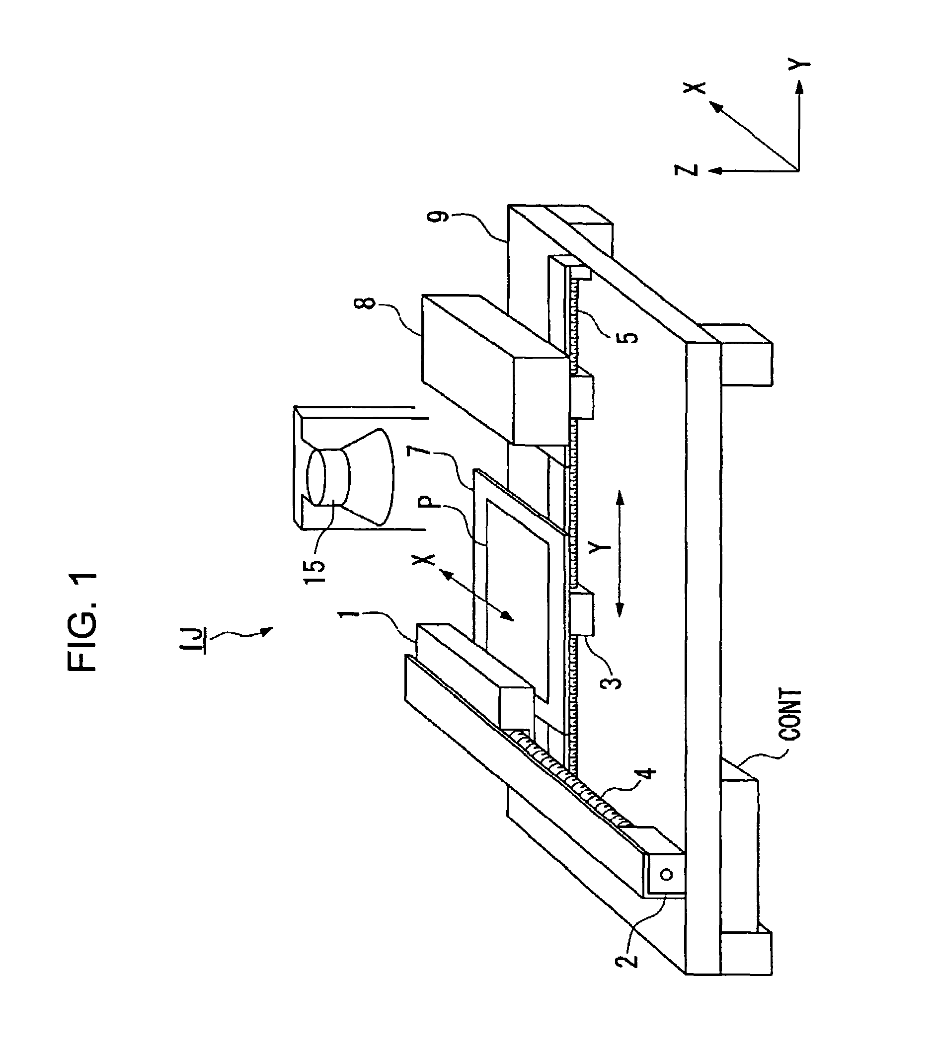
[0037]Referring to FIG. 1 to FIG. 12, embodiments of a device, a method of manufacturing the same, an electro-optic device and electronic equipment according to the present invention will be described.

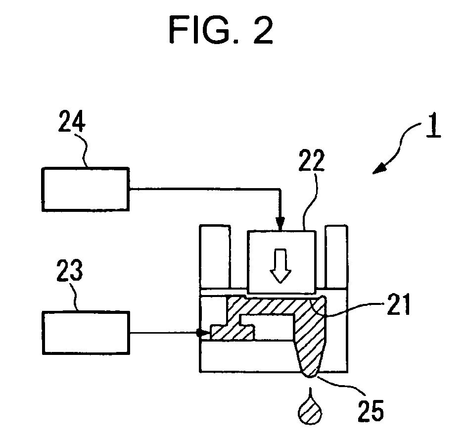
[0038]Here, ink for a wiring pattern, which is functional fluid, will be described.

[0039]Ink for a wiring pattern discharged in the form of liquid drops from a nozzle of a liquid drop discharging head by a liquid drop discharging process is generally formed of dispersion liquid obtained by dispersing conductive fine particles in a dispersion medium.

[0040]In the present embodiment, in addition to metal fine particles containing any one of gold, silver, copper, palladium, and nickel, oxide of the same, conductive polymer, and superconductive fine particles may be employed as the conductive fine particles.

[0041]These conductive fine particles may be used by being coated with organic substance on the surface thereof in order to improve its dispersion property. As a coating agent to be coat...


PUM

PropertyMeasurementUnit
surface tensionaaaaaaaaaa
viscosityaaaaaaaaaa

Abstract

A first conductive film is formed on a wiring pattern area on a plate by dropping liquid drops. A second conductive film which is electrically separated from the first conductive film is formed by discharging liquid drops outside of the wiring pattern area on the plate.

Description

RELATED APPLICATIONS[0001]This application claims priority to Japanese Patent Application Nos. 2003-085539 filed Mar. 26, 2003 and 2004-035081 filed Feb. 12, 2004 which are hereby expressly incorporated by reference herein in their entireties.BACKGROUND[0002]1. Technical Field[0003]The present invention relates to a device, a method of manufacturing the same, an electro-optic device, and electronic equipment.[0004]2. Background Art[0005]Wiring used for electronic circuits or integrated circuits is manufactured, for example, by a photolithography method. In the photolithography method, the wiring is formed by applying photosensitive material called resist on a plate, on which a conductive film is applied in advance, developing by irradiating a circuit pattern, and etching the conductive film according to a resist pattern. The lithography method requires large scale equipment and complex processes such as a vacuum device, and the material usage efficiency is only several percent. Ther...

Claims


Application Information

Patent Timeline
Patent Type & Authority Patents(United States)
IPC IPC(8): B32B3/00B32B7/12G02F1/1345B05C5/00G09F9/00H01J9/02H01J11/22H01J11/32H01J11/34H01J31/12H01L21/02H01L21/288H01L21/3205H01L21/768H01L23/52H01L23/522H01L51/50H05B33/10H05K3/12
CPCH01J9/02H05K3/125H05K2201/09781Y10T428/24917Y10T428/2809Y10T428/2804H05K2203/013B32B21/04E04C2/24
Inventor HIRAI, TOSHIMITSU
Owner SEIKO EPSON CORP
Why Eureka
Try Eureka