
Thin film capacitor and its manufacture method

a thin film capacitor and manufacturing method technology, applied in the field of capacitors, can solve the problems of high leak current, difficult to reduce inductance, and severe approach to use laminated ceramic capacitors, and achieve the effects of reducing power source noise, high capacitance, and low inductan

Inactive Publication Date: 2008-02-05
FUJITSU LTD
View PDF25 Cites 1 Cited by
  • Summary
  • Abstract
  • Description
  • Claims
  • Application Information

AI Technical Summary

Benefits of technology

The present invention provides a thin film capacitor with a single crystal high dielectric constant dielectric layer that has low inductance and high capacitance suitable for use in reducing power source noises and the like of a large scale integrated circuit operating at a high frequency. The method of manufacturing the thin film capacitor involves epitaxially growing layers on a single crystal silicon substrate and forming an upper electrode layer above the single crystal high dielectric constant dielectric layer. The technical effects of this invention include improved performance and reliability of thin film capacitors in high-frequency applications.

Problems solved by technology

Although a large capacitance can be obtained, it is not easy to reduce inductance because the electrode layers are connected to the surface electrodes at the sides of the electrode layers.
However, an approach of using laminated ceramic capacitors is severe.
If there is any defect in a thin dielectric layer, leak current is likely to increase.
As compared with a laminated ceramic capacitor, it is more difficult to form a thin film capacitor of a multilayer structure.
Under these circumstances, it is not easy to form a thin film capacitor of large capacitance, as compared with a laminated ceramic capacitor.
Leak current is likely to flow through a grain boundary, and deteriorates the leak characteristics of the dielectric layer, i.e., its breakdown voltage.
As the surface of the dielectric layer becomes more irregular, the uniformity of an electric field is degraded and an electric field concentration occurs, resulting also in deterioration of the leak characteristics or breakdown voltage.
However, it is difficult to form such a single crystal substrate which is inexpensive and has a large area.

Method used


Image

  • Thin film capacitor and its manufacture method
  • Thin film capacitor and its manufacture method
  • Thin film capacitor and its manufacture method

Examples


Embodiment Construction

[0038]The present inventors have found that a single crystal lower electrode and a single crystal dielectric layer can be formed on a single crystal silicon substrate.

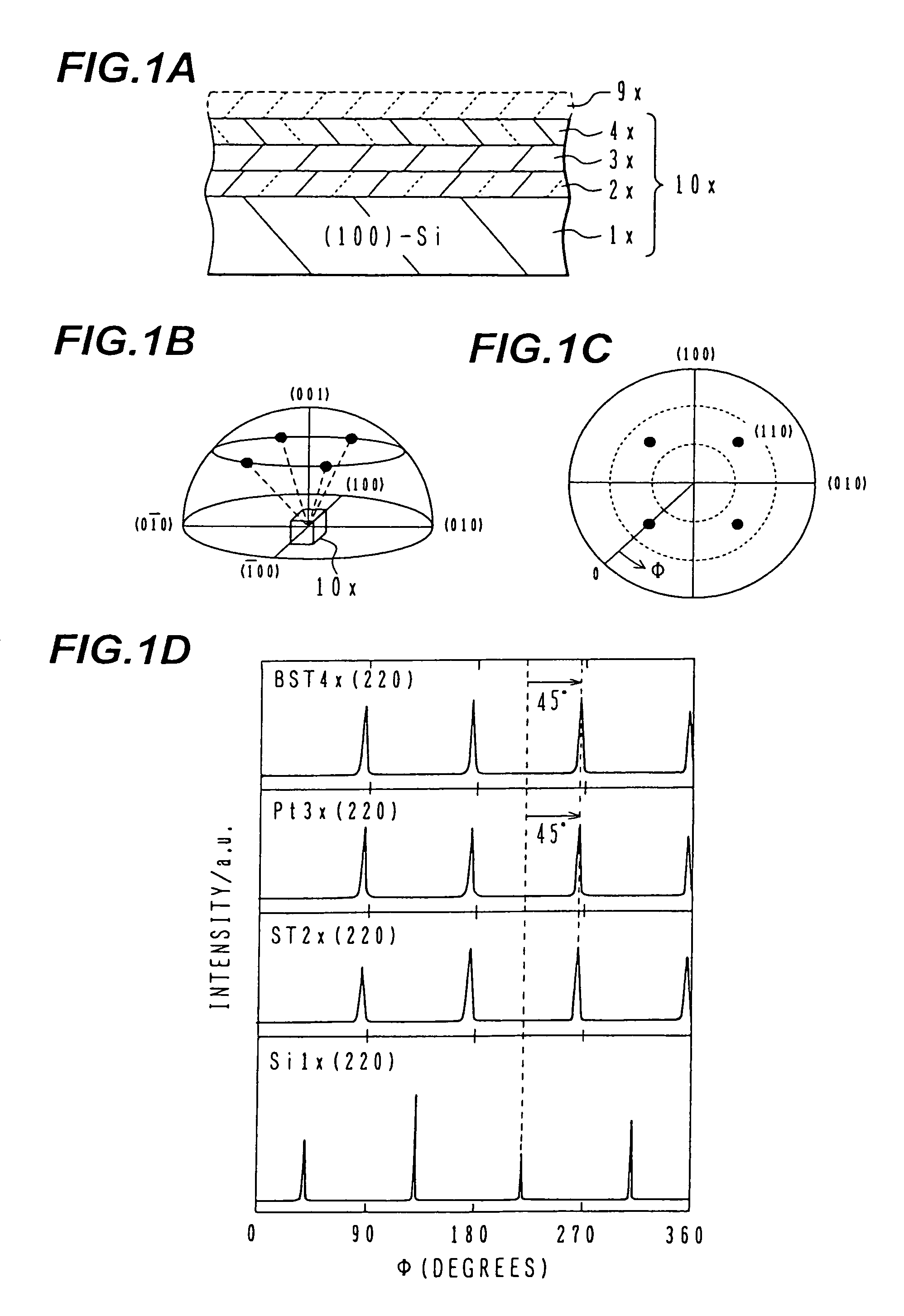
[0039]FIG. 1A shows the structure of a sample. A silicon substrate 1x is prepared having the (100) plane. An SrTiO3 film 2x of about 100 nm in thickness to be used as an intermediate layer of insulating material is formed on the (100) plane of the silicon substrate by RF sputtering in an Ar / O2 atmosphere containing Ar and O2 at a substrate temperature of 800° C., by using an SrTiO3 sputtering target.

[0040]A Pt layer 3x of about 500 nm to be used as a lower electrode layer is formed on the intermediate layer 2x by DC sputtering in an Ar atmosphere at a substrate temperature of 600° C., and on the Pt layer 3x, a BaSrTi3 layer 4x of about 50 nm in thickness made of high dielectric constant perovskite oxide is formed by RF sputtering in an Ar / O2 atmosphere. A sample 10x was formed in this manner and it was verified through...


PUM

PropertyMeasurementUnit
dielectric constantaaaaaaaaaa
thicknessaaaaaaaaaa
thicknessaaaaaaaaaa

Abstract

A thin film capacitor is provided which includes a single crystal high dielectric constant dielectric layer. The thin film capacitor has a single crystal silicon substrate, a single crystal intermediate layer epitaxially grown on the single crystal silicon substrate, a single crystal lower electrode epitaxially grown on the single crystal intermediate layer, a single crystal high dielectric constant dielectric layer epitaxially grown on the lower electrode layer, an upper electrode layer formed above the single crystal high dielectric constant dielectric layer, and a plurality of conductor terminals connected to the lower electrode layer and upper electrode layer at a plurality of positions.

Description

CROSS REFERENCE TO RELATED APPLICATION[0001]This application is a continuation application of an International patent application PCT / JP03 / 10392, filed on Aug. 15, 2003, which is based upon and claims the benefit of priority of Japanese patent application 2002-251267, filed on Aug. 29, 2002, the entire contents of both of which are incorporated herein by reference.BACKGROUND OF THE INVENTION[0002]A) Field of the Invention[0003]The present invention relates to a capacitor, and more particularly to a capacitor of low inductance and large capacitance suitable for being used as a decoupling capacitor for absorbing noises generated in a large scale integrated circuit (LSI) operating at a high frequency.[0004]In the present specification, a relative dielectric constant of 10 or larger is called a high dielectric constant.[0005]B) Description of the Related Art[0006]A capacitor is an important constituent element in a large scale integrated circuit (LSI) operating at a high frequency. For ...

Claims


Application Information

Patent Timeline
Patent Type & Authority Patents(United States)
IPC IPC(8): H01L29/94H01L21/44H01G4/33H01L21/02H01L21/822H01L27/04H01L27/06H01L27/08H10B12/00
CPCH01G4/33H01L27/0629H01L27/0805H01L28/40H01L27/02H10B12/00
Inventor KURIHARA, KAZUAKISHIOGA, TAKESHIBANIECKI, JOHN DAVID
Owner FUJITSU LTD
Learn More