LED illumination device with layered phosphor pattern

a technology of phosphor coating and illumination device, which is applied in the direction of discharge tube/lamp details, discharge tube luminescent screen, discharge tube/lamp details, etc., can solve the problems of significant radiation emitted from the die that bleeds through the phosphor coating, light bleed-through disturbs the lamp color, and the effect of reducing each of these problems

Active Publication Date: 2008-02-05
GE LIGHTING SOLUTIONS LLC
View PDF9 Cites 77 Cited by
  • Summary
  • Abstract
  • Description
  • Claims
  • Application Information

AI Technical Summary

Benefits of technology

[0007]In accordance with a first aspect of the present exemplary embodiments, there is provided a method of forming a light emitting device including depositing a first phosphor material over a semiconductor light emitter and depositing a second phosphor material over the first phosphor material, wherein the first phosphor material has at least one of a shorter decay time and a lower absorption of radiation from the semiconductor light emitter than the second phosphor material.
[0008]In accordance with a second aspect of the present exemplary embodiment, there is provided a light emitting device including a semiconductor light emitter and at least two phosphor materials. The first phosphor material is disposed closer to the light emitting diode or laser diode than a second phosphor material. The second phosphor material is selected to have a decay time greater than the decay time of the first phosphor material. Alternatively, the first phosphor material can demonstrate a lesser efficiency to absorb the light emitted by the light emitting diode or laser than the second phosphor material.
[0009]In accordance with a third aspect of the present exemplary embodiments, there is provided a light emitting device including a light emitting diode or laser emitting diode and at least two phosphor materials, wherein a first phosphor material is positioned such that radiation emitted from the light emitting diode or laser emitting diode strikes the first phosphor material prior to striking the second phosphor material, and further wherein the first phosphor material has at least one of a shorter decay time and a lower absorption of radiation emitted from the light emitting diode or laser emitting diode than the second phosphor material.

Problems solved by technology

However, the potential for general illumination is also enormous.
There are three primary problems in the white LED lamps described above, which are particularly present in UV-LED devices.
First, if the absorption of the phosphor at the emitted UV wavelength is not high, then there is a significant amount of radiation emitted from the die that bleeds through the phosphor coating.
Similarly, too much blue light bleed-through disturbs the lamp color.
Second, for phosphors with slow decay times (>3 ms), the high fluxes present in the UV-LED device can lead to non-linear quenching effects from large excited steady state population.
Third, the heating of the phosphor particles situated immediately on top of or adjacent the LED chip by the LED leads to reduced efficiency (a phenomenon known as thermal quenching).

Method used


Image

  • LED illumination device with layered phosphor pattern
  • LED illumination device with layered phosphor pattern
  • LED illumination device with layered phosphor pattern

Examples


Embodiment Construction

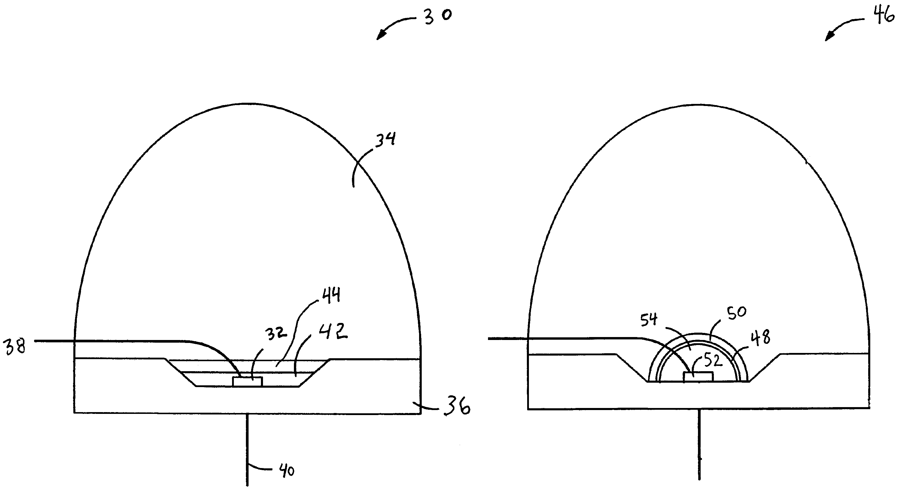
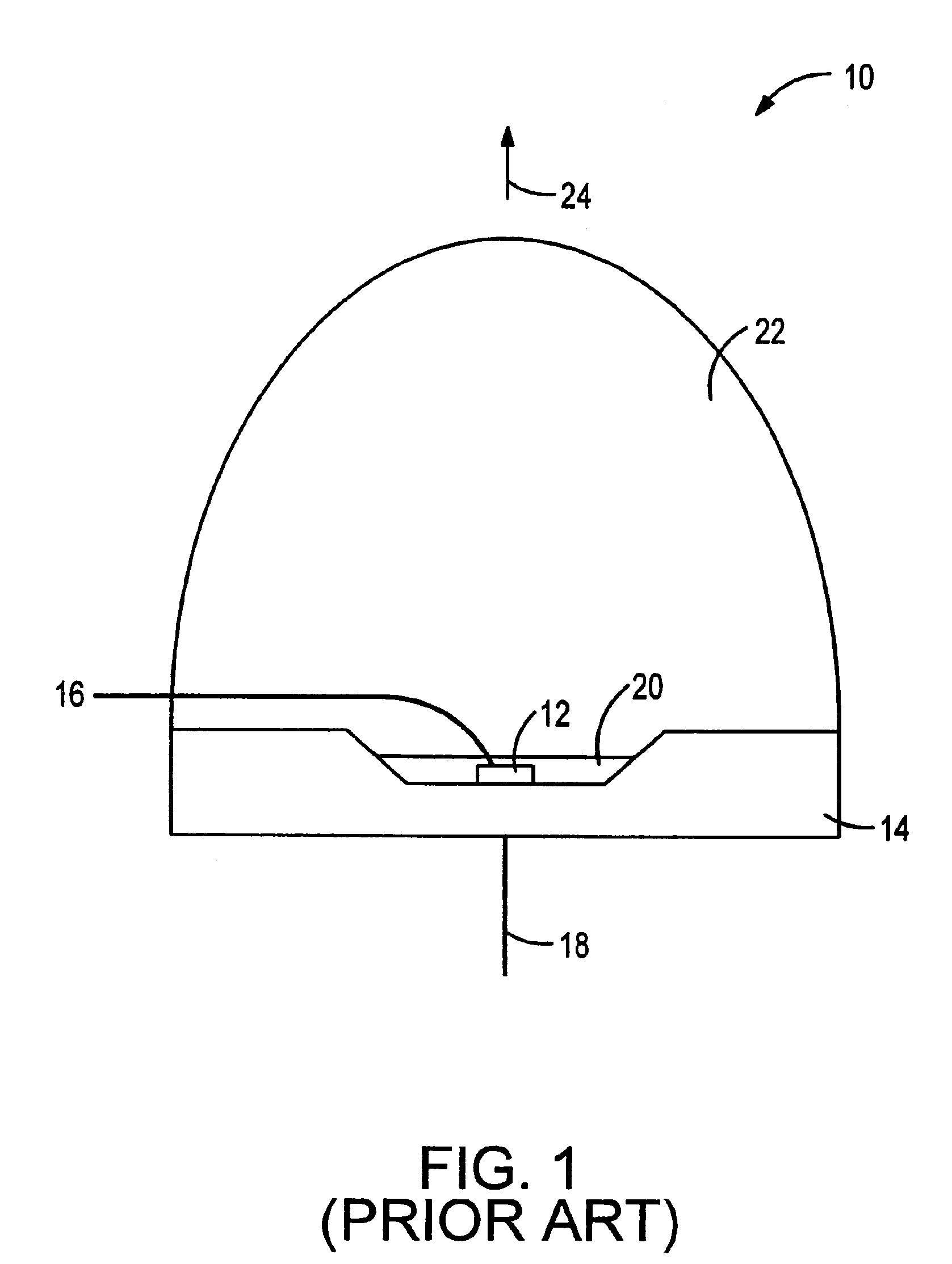
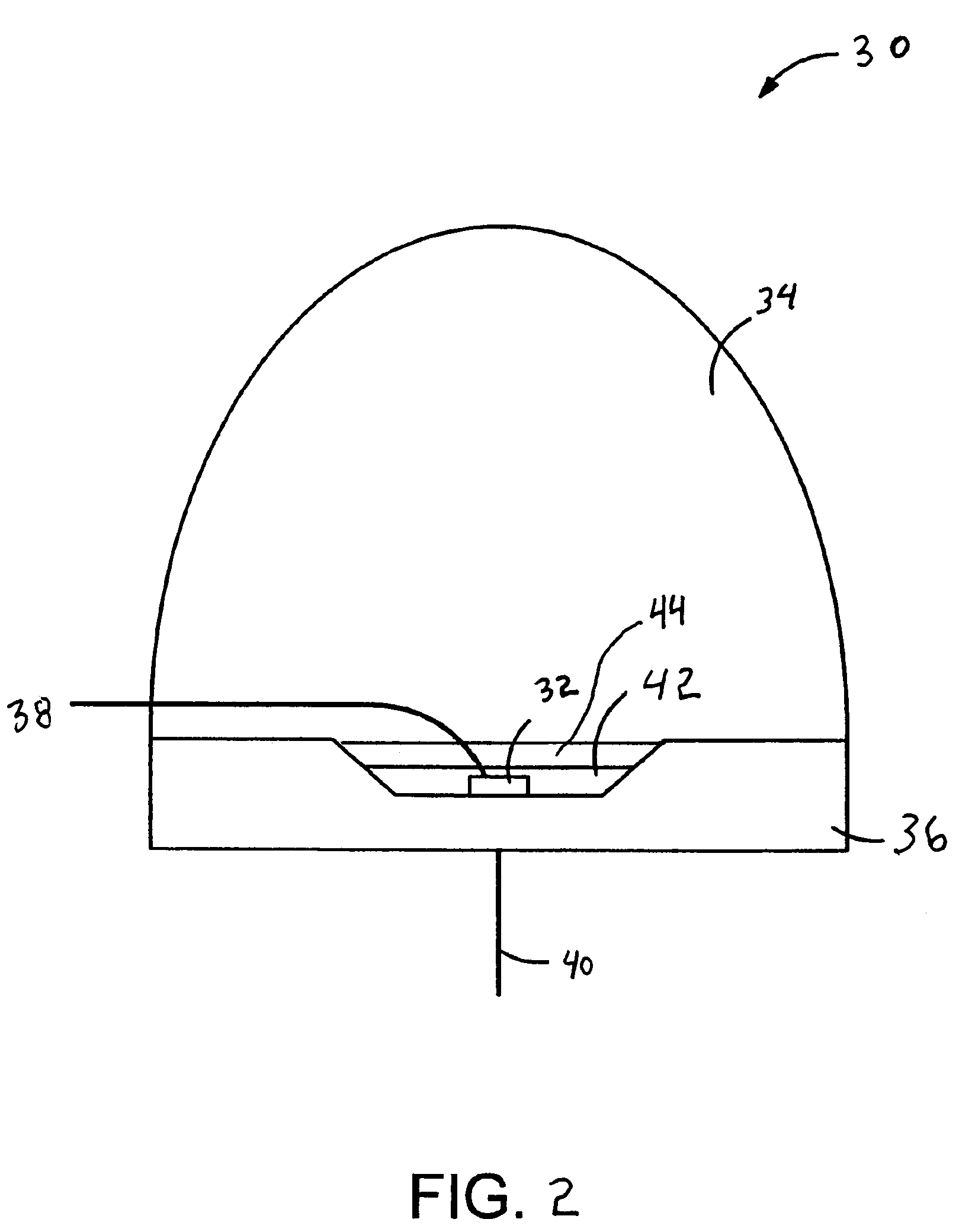
[0017]With reference to FIG. 1, an exemplary phosphor-conversion light emitting device or lamp 10 is shown. The light emitting device 10 comprises a semiconductor UV or blue radiation source, such as a light emitting diode (LED) chip or die 12 and leads 14 electrically attached to the LED chip. The leads 14 may comprise thin wires supported by a thicker lead frame(s) 16 or the leads may comprise self supported electrodes and the lead frame may be omitted. The leads 14 provide current to the LED chip 12 and thus cause the LED chip 12 to emit radiation. The die 12 is covered by a phosphor containing layer 20.

[0018]The phosphor containing layer 20 may contain a phosphor material and an encapsulant. The encapsulant is preferably an epoxy, plastic, low temperature glass, polymer, thermoplastic, thermoset material, resin or other type of LED encapsulating material as is known in the art. Optionally, the encapsulant is a spin-on glass or some other high index of refraction material. Prefer...


PUM

PropertyMeasurementUnit
mean particle sizeaaaaaaaaaa
luminescence decay timeaaaaaaaaaa

Abstract

A method of applying at least two phosphors to an LED, wherein a first phosphor material having a lower absorption, shorter luminescence decay time, and / or lower thermal quenching than a second phosphor material is positioned closer to the LED than the second phosphor. Such an arrangement provides a light emitting device with improved lumen output and color stability over a range of drive currents.

Description

BACKGROUND[0001]The present exemplary embodiments relate to a method for layering phosphors in a light emitting diode (“LED”) device to minimize non-radiative loss mechanisms in the phosphor layer. It finds particular application in conjunction with LEDs, and will be described with particular reference thereto. However, it is to be appreciated that the present exemplary embodiment is also amenable to other like applications.[0002]Light emitting diodes (“LEDs”) are well-known solid state devices that can generate light having a peak wavelength in a specific region of the light spectrum. LEDs are typically used as illuminators, indicators and displays. However, the potential for general illumination is also enormous. Originally, the most efficient LEDs emitted light having a peak wavelength in the red region of the light spectrum, i.e., red light. However, a type of LED based on a gallium nitride (GaN) die has also been developed that can efficiently emit light having a peak wavelengt...

Claims


Application Information

Patent Timeline
Patent Type & Authority Patents(United States)
IPC IPC(8): H05B33/00C09K11/66C09K11/77H01J1/62H01J63/04H01L21/00H01L33/50
CPCC09K11/665C09K11/7734C09K11/7739C09K11/774C09K11/7774H01L33/504H01L2933/0041
Inventor SETLUR, ANANT ACHYUTSHIANG, JOSEPH JOHNSRIVASTAVA, ALOK MANICOMANZO, HOLLY ANNWEAVER, STANTON EARLBECKER, CHARLES ADRIAN
Owner GE LIGHTING SOLUTIONS LLC
Why Eureka
Try Eureka