
Display device and an electronic apparatus using the same

a display device and electronic equipment technology, applied in the field of display devices, can solve the problems of increasing the number of components, reducing the mechanical reliability of the tablet pc, reducing the volume and cost of the portable telephone set, etc., to reduce the volume and cost, and reduce the mechanical reliability

Inactive Publication Date: 2008-02-05
SEMICON ENERGY LAB CO LTD
View PDF24 Cites 41 Cited by
  • Summary
  • Abstract
  • Description
  • Claims
  • Application Information

AI Technical Summary

Benefits of technology

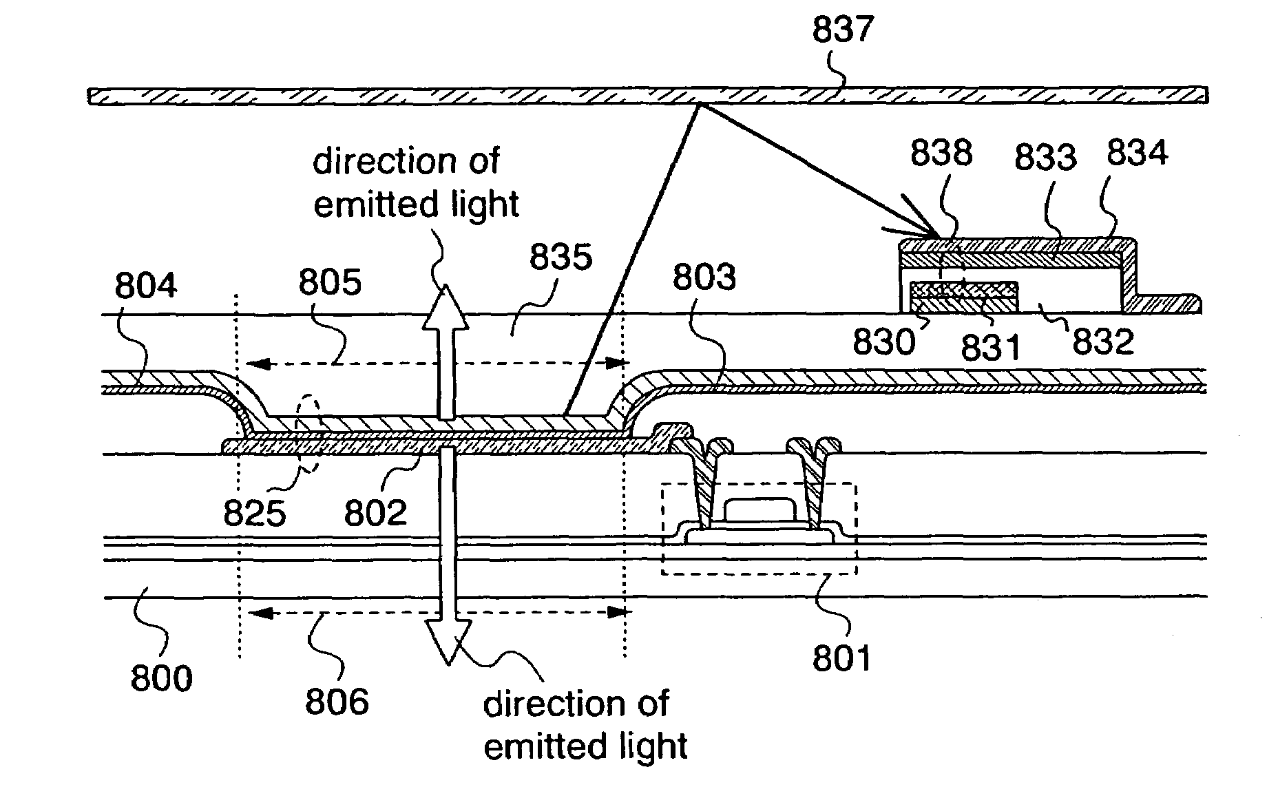
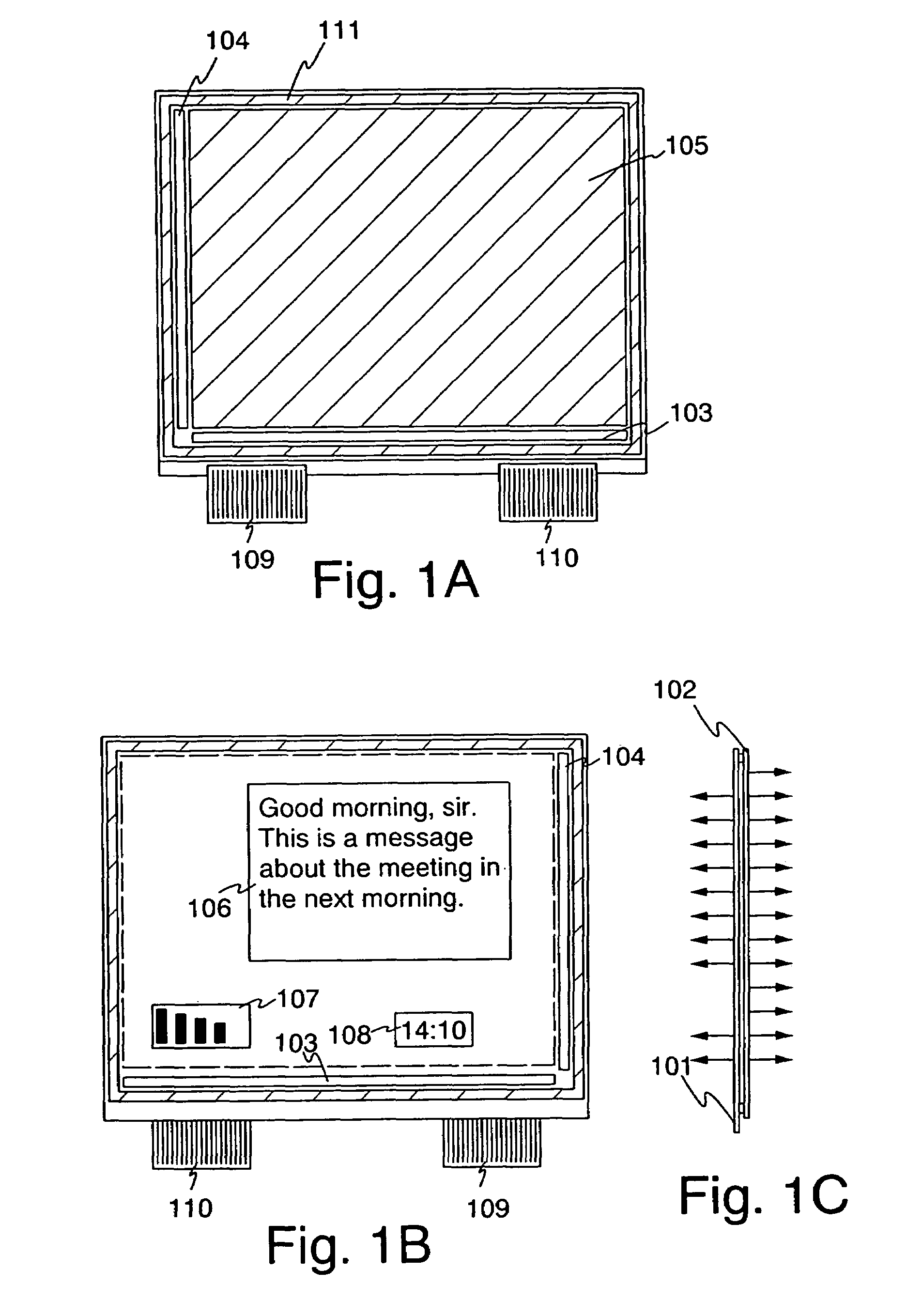
The invention provides a display device with two display surfaces, which allows for better mechanical reliability and reduces the number of components and volume. The display device uses a dual emission display, which allows for a high reliability without using a complicated axis of rotation. The display device also includes a detecting means for detecting the angle between the two housings and a switching means for changing the scan direction of the display means. The invention also provides an electronic apparatus with a display screen, such as a personal computer, video camera, or portable communication tool. The electronic apparatus may also include an electrical storage means and a light emission control means for lighting or flashing the display screen.

Problems solved by technology

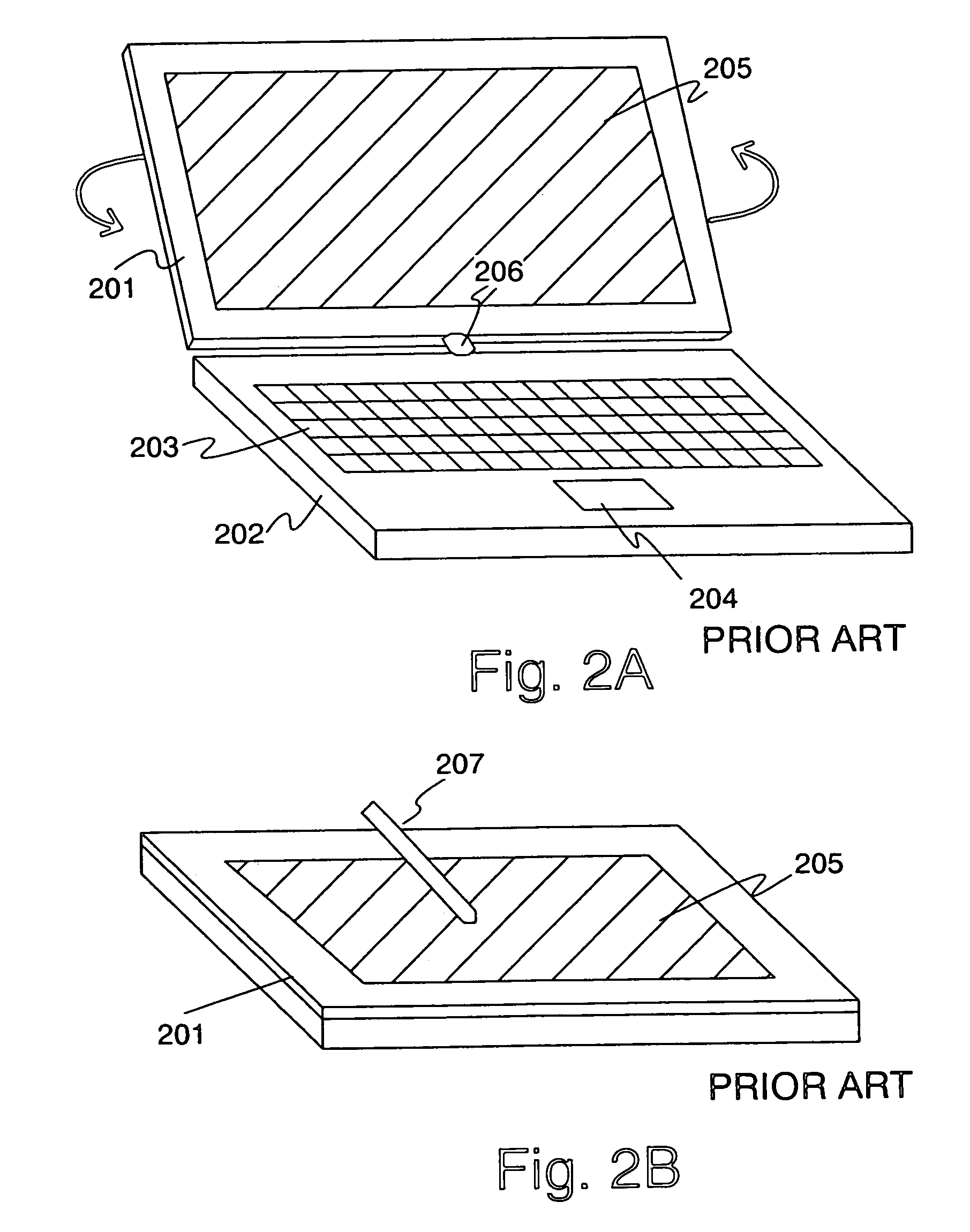
Therefore, mechanical reliability of the tablet PC is lowered as compared with a PC using a simple hinge, thus machine life is shortened.
In the above-described portable telephone set comprising both a main display and a sub-display, control circuits for controlling each of the displays are necessarily provided, leading to the increase in the number of components, and the increase in volume and cost of the portable telephone set.
Further, the two displays make the first housing thicker and also increase the volume of the portable telephone set.

Method used


Image

  • Display device and an electronic apparatus using the same
  • Display device and an electronic apparatus using the same
  • Display device and an electronic apparatus using the same

Examples


embodiment 1

[0077]With reference to FIG. 6, explanation will be made on a source signal line driver circuit used for the display devices of the invention. Since images are displayed on both sides of the display device in the invention, the images are displayed in opposite directions viewing from the opposite side. Therefore, the driving direction of the screen has to be changed depending on the direction from which the screen is viewed. Thus, in the display device of the invention, a source signal line driver circuit is formed as shown in FIG. 6.

[0078]A source signal line driver circuit shown in FIG. 6 comprises a shift register 601, a NAND circuit 607, a buffer circuit 608, and analog switches 609 to 612. The operation is explained hereinafter. The shift register 601 is formed with a series of DFFs 602, each of which comprises clocked inverters 603 and 604 and an inverter 605. A signal is input to the DFF 602 from a terminal SSP and transferred to the subsequent DFF 602 by clock signals (CL an...

embodiment 2

[0081]FIGS. 15A and 15B show an example of a light emitting display device using time gray scale. FIG. 15A shows a pixel for driving a light emitting element 1503 by using time gray scale. The pixel comprises a driving TFT 1502, a storage capacitor 1505 and a switching TFT 1501 as well as the light emitting element 1503. A gate of the switching TFT 1501 is connected to a gate signal line G1. When the gate signal line G1 is high, the switching TFT 1501 is turned ON and data on a source signal line S1 is written to the storage capacitor 1505 and a gate of the driving TFT 1502. When the driving TFT 1502 is turned ON, a current is supplied from a power supply line V1 to the light emitting element 1503 through the driving TFT 1502. This state is held until the next writing is done.

[0082]FIG. 15B is a timing chart of time gray scale. In this embodiment, 4-bit time gray scale is taken as an example, though the invention is not exclusively limited to 4-bit. One frame is composed of four sub...

embodiment 3

[0086]FIGS. 16A and 16B show an example of a light emitting display device using time gray scale. FIG. 16A shows a pixel for driving a light emitting element 1603 by using time gray scale. The pixel comprises a driving TFT 1602, an erasing TFT 1606, a storage capacitor 1605 and a switching TFT 1601 as well as the light emitting element 1603. A gate of the switching TFT 1601 is connected to a gate signal line G1. When the gate signal line G1 is high, the switching TFT 1601 is turned ON, and data on a source signal line S1 is written to the storage capacitor 1605 and a gate of the driving TFT 1602. When the driving TFT 1602 is turned ON, a current is supplied from a power supply line V1 to the light emitting element 1603 through the driving TFT 1602. This state is held until the next writing is done.

[0087]FIG. 16B is a timing chart of time gray scale. In this embodiment, 4-bit time gray scale is taken as an example, though the invention is not exclusively limited to 4-bit. One frame i...


PUM


Abstract

In a conventional display device comprising a sub-display, the display device is increased in thickness and in the number of components as the number of displays is increased. In the present invention, a dual emission display device is used so that either surface of a display is used as a main display or a sub-display. Accordingly, the display device can be reduced in thickness and in the number of components. Further, mechanical reliability can be enhanced when the invention is applied to a tablet PC, a video camera and the like.

Description

BACKGROUND OF THE INVENTION[0001]1. Field of the Invention[0002]The present invention relates to a display device having a display screen which is formed on a flat plate surface by using a light emitting element typified by an electro luminescence element, and more particularly relates to an electronic apparatus using the display device.[0003]2. Description of Related Art[0004]In recent years, with the development in communication technologies, portable telephone sets have been widely used. In future, transmission of moving pictures and transmission of a large volume of information are expected. On the other hand, through reduction in weight of personal computers (PCs), those adapted for mobile communication have been produced. Information terminals called PDA originated in electronic notebooks have also been produced in large quantities and widely used. In addition, with the advance of display devices, most of those portable information apparatuses are equipped with a flat panel di...

Claims


Application Information

Patent Timeline
Patent Type & Authority Patents(United States)
IPC IPC(8): G09G3/30H01J1/62G02B5/20G09F9/30G09F9/40G09G5/393G09G5/395H01L27/146H01L27/32H01L51/50H05B33/00
CPCG06F3/1423G09G3/3258G09G5/393G09G5/395F21V9/14F21V21/00G09G3/30G09G3/2022G09G3/3266G09G2300/023G09G2300/0842G09G2310/0251G09G2340/0492G09G2360/14G09G2360/142H01L27/14678H01L27/3244H01L27/3269H01L2251/5323H10K59/12H10K59/13H10K2102/3031H10K2102/301
Inventor YAMAZAKI, SHUNPEIKOYAMA, JUN
Owner SEMICON ENERGY LAB CO LTD
Learn More