Smooth metal semiconductor surface and method for making the same

a metal layer and substantially smooth technology, applied in semiconductor devices, semiconductor/solid-state device details, electrical devices, etc., can solve the problems of affecting the operation of a device, the breakdown of the junction within the device the breakdown of the junction at a relatively low voltage, so as to reduce the mean surface roughness of the metal layer, reduce current, and consume less power

Inactive Publication Date: 2008-02-12
MONTEREY RES LLC
View PDF17 Cites 5 Cited by
  • Summary
  • Abstract
  • Description
  • Claims
  • Application Information

AI Technical Summary

Benefits of technology

[0020]There may be several advantages for reducing the mean surface roughness of a metal layer as described herein. For example, metal layers with substantially smooth surfaces may allow a junction within a MRAM device formed therefrom to breakdown at a higher voltage than in an embodiment in which the junction is formed from layers with relatively rough surfaces. In particular, a MRAM device with substantially smooth layers below a tunneling layer of a magnetic tunneling junction (MTJ) may allow a substantially even and smooth tunneling layer to be formed, thereby preventing the junction from breakdown at a lower voltage. Consequently, the process window at which a MRAM device may be operated may be made larger by the inclusion of substantially smooth surfaces. As a result, the device may be operated at a lower current and consume less power. In addition or alternatively, the reliability and endurance of a device may be increased by the inclusion of smooth surfaces within the device. Furthermore, producing a substantially smooth metal layer may aid in producing substantially smooth layers above the metal layer, since the overlying layers will not conform to a relatively rough surface. Moreover, in the embodiment in which a fill layer is used to fill the valleys of the metal layer associated with the surface roughness of the metal layer, the method may reduce or eliminate the removal of the metal layer. In such an embodiment, the metal layer may be deposited within the design specifications of the device.

Problems solved by technology

In some cases, the surface roughness of one or more layers within a semiconductor topography may affect the operation of a device formed from such a topography.
For example, in cases including magnetic random access memory (MRAM) devices, layers with relatively rough surfaces may undesirably cause a junction within a device to breakdown at a relatively low voltage.
In particular, relatively rough surfaces of layers within MRAM devices including magnetic tunneling junctions (MTJ) may cause a breakdown of the junction at a low voltage.
In some cases, breakdown at a relatively low voltage may cause the device to frequently malfunction, thereby decreasing the reliability and / or yield of the device.
In addition or alternatively, the threshold voltage by which the device is activated may be lower and thus, the junction breakdown may inhibit the entire operation of the device in some cases.
Since tunneling layers within MTJs are typically very thin (e.g., approximately 15 angstroms or less), the unevenness of such a layer may be caused by relatively rough surfaces of underlying layers.
Conventional deposition processes, however, have limited capability to produce layers with substantially smooth surfaces.
Moreover, the accumulation of layers with such surface roughnesses may cause an upper layer to have an even greater surface roughness than may be produced by a particular deposition technique.

Method used


Image

  • Smooth metal semiconductor surface and method for making the same
  • Smooth metal semiconductor surface and method for making the same
  • Smooth metal semiconductor surface and method for making the same

Examples


Embodiment Construction

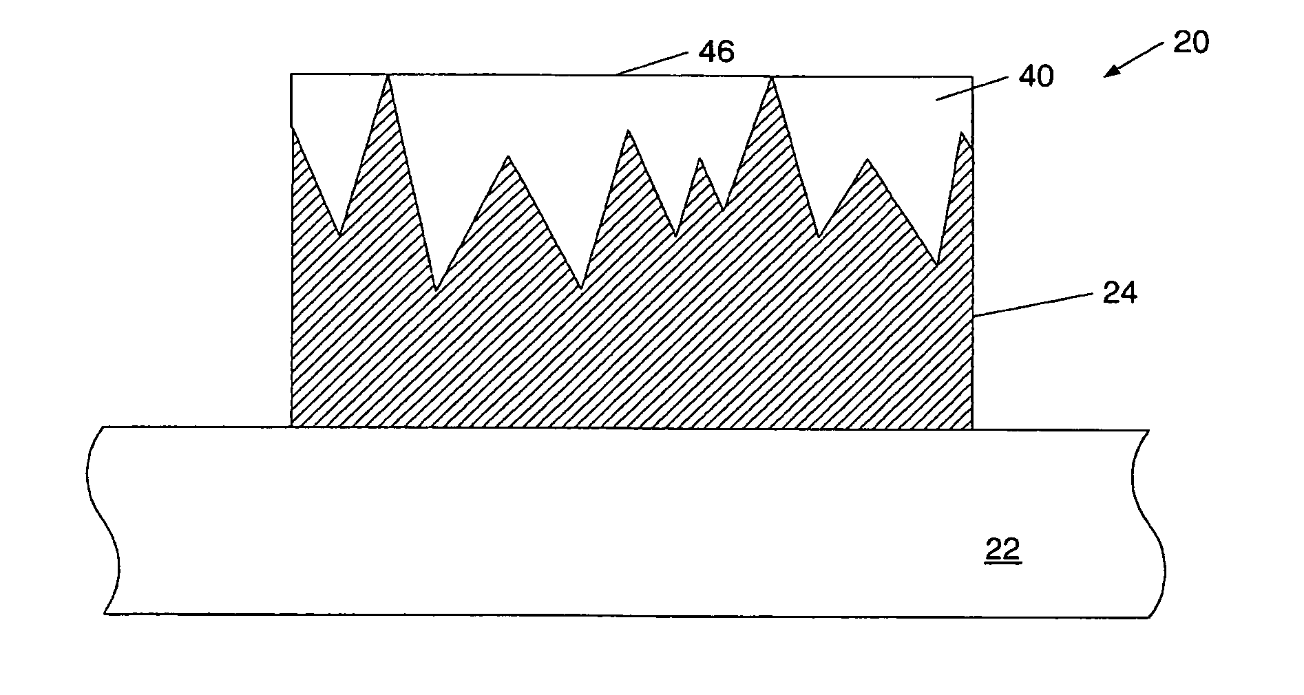
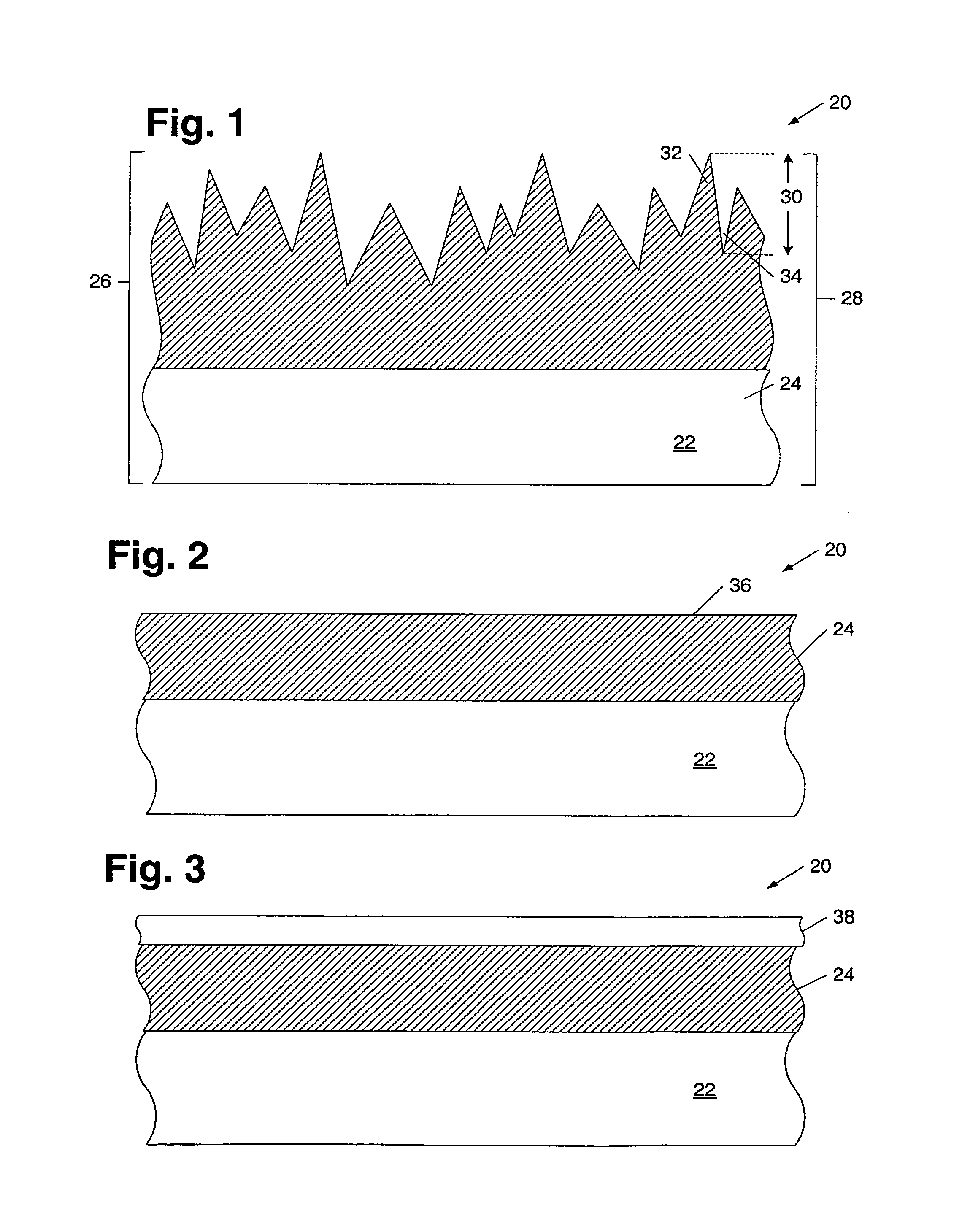
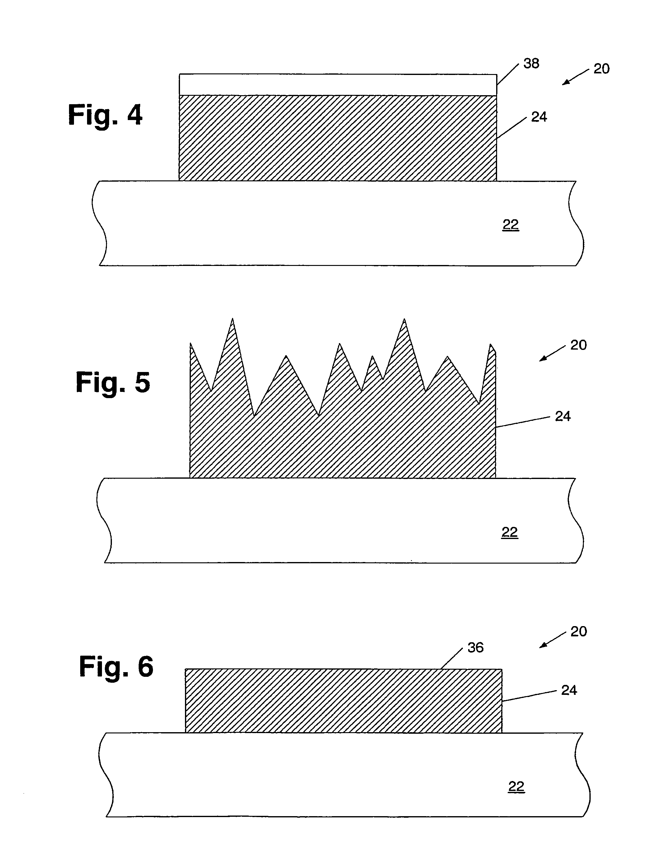
[0036]Turning to the drawings, exemplary embodiments of methods for processing a semiconductor topography are shown in FIGS. 1-11. In particular, methods for reducing the mean surface roughness of a metal layer are provided. FIG. 1 depicts a partial cross-sectional view of semiconductor topography 20 in which metal layer 24 is arranged upon semiconductor layer 22. The upper portion of metal layer 24 is shown with a plurality of peaks and valleys representing the surface roughness of the layer. It is noted that the peaks and valleys are greatly exaggerated with respect to the thickness of the layer to emphasize the roughness of the layer prior to the application of the smoothening process described herein. In general, the mean surface roughness of metal layer 24 may be on the order of one hundred or a few hundred angstroms while the thickness of metal layer 24 may be between a few hundred angstroms and a few thousand angstroms. The measurement of the surface roughness of a layer is d...


PUM

PropertyMeasurementUnit
surface roughnessaaaaaaaaaa
thicknessaaaaaaaaaa

Abstract

A method for reducing the surface roughness of a metal layer is provided. In some embodiments, the method may include polishing the metal layer to a level substantially above any layers arranged directly beneath the metal layer. In some cases, the semiconductor topography comprising the metal layer may be substantially absent of any material laterally adjacent to the metal layer during polishing. In either case, a semiconductor topography having a metal layer with a mean surface roughness less than the mean surface roughness obtained during the deposition of the metal layer may be obtained. As such, the method may include reducing the mean surface roughness of a metal layer. For example, the method may include reducing the mean surface roughness of a metal layer by at least a factor of ten.

Description

[0001]This application is a divisional application from prior application Ser. No. 10 / 113,309 filed Mar. 29, 2002, now U.S. Pat. No. 6,740,588.BACKGROUND OF THE INVENTION[0002]1. Field of the Invention[0003]This invention relates to semiconductor device manufacturing, and more particularly, to a method for fabricating a metal layer with a substantially smooth surface.[0004]2. Description of the Related Art[0005]The following descriptions and examples are not admitted to be prior art by virtue of their inclusion within this section.[0006]In most cases, a material may include a plurality of peaks and valleys upon its surface, which are associated with the surface roughness of the material. Such peaks and valleys may be visible by the naked eye or through an optical microscope, an electron microscope, or an atomic force microscope (AFM). In either embodiment, the surface roughness of a material may be characterized by the vertical distances between the bases of valleys and crests of th...

Claims


Application Information

Patent Timeline
Patent Type & Authority Patents(United States)
IPC IPC(8): H01L21/82H01L21/321H01L21/768H01L27/22
CPCH01L21/3212H01L21/7684H01L27/222H10B61/00
Inventor KOUTNY, JR., WILLIAM W. C.
Owner MONTEREY RES LLC
Why Eureka
Try Eureka