High frequency power amplifier circuit

a power amplifier and circuit technology, applied in the field of high frequency power amplifier circuits, can solve the problems of difficult to difficult to miniaturize the module, and large power loss, so as to improve the detection sensitivity of output power, prevent excessive output power from becoming excessive, and reduce the size of the modul

Active Publication Date: 2008-02-19
MURATA MFG CO LTD
View PDF5 Cites 61 Cited by
  • Summary
  • Abstract
  • Description
  • Claims
  • Application Information

AI Technical Summary

Benefits of technology

[0009]An object of the present invention is to provide an output power detection circuit capable of obtaining sufficient detection output even in a range where a requested output power level is low in a radio communication system which detects output power and performs a feedback control.
[0013]In output power detection circuit which detects a level of an output power on the basis of an AC signal received from an output part (from the final amplification stage to an output terminal) of a high frequency power amplifier circuit via a coupling capacitor, on the basis of output power control voltage and reference voltage, in a state where output power control voltage is lower than a predetermined level, current according to the output power control voltage is generated and supplied to the output power detection circuit, and the detection sensitivity of the output power detection circuit improves according to the supplied current.
[0014]More concretely, the output power detection circuit includes: a transistor for output detection which receives, by its control terminal, an alternate current signal supplied from the output part of the high frequency power amplifier circuit via the coupling capacitor and makes current proportional to the output power flow; a bias generating circuit for giving an operation point to a control terminal of the transistor; a current mirror circuit for transferring current flowing in the transistor for output detection; and a current-voltage converting circuit for converting the transferred current to voltage. In addition, a current generating circuit for generating output power control voltage is provided. By making the generated current flow to the current-voltage converting circuit in the output power detection circuit, the detection sensitivity of the output power detection circuit in a state where the output power control voltage is low is improved.

Problems solved by technology

A number of semiconductor integrated circuits and electronic parts separate from the high frequency power amplifier circuit are used, so that it is difficult to reduce the size of the module.
When the coupler is used, there is an inconvenience such that a power loss is relatively large.
Consequently, it becomes more difficult to miniaturize the module.
Second, the circuit is to be highly sensitive.
Third, an insertion loss of the circuit is to be low.
Fifth, the circuit should not make abnormal current flow to the power amplifier circuit due to mismatch between an actual output state of the power amplifier circuit and output control by feedback control, causing destruction of the power amplifier circuit.
The conventional detecting method using a coupler meets the demands of the second, fourth, and fifth characteristics more or less but does not sufficiently address the requirements on the miniaturization of the first characteristic and the low insertion loss of the third characteristic.

Method used


Image

  • High frequency power amplifier circuit
  • High frequency power amplifier circuit
  • High frequency power amplifier circuit

Examples


first embodiment

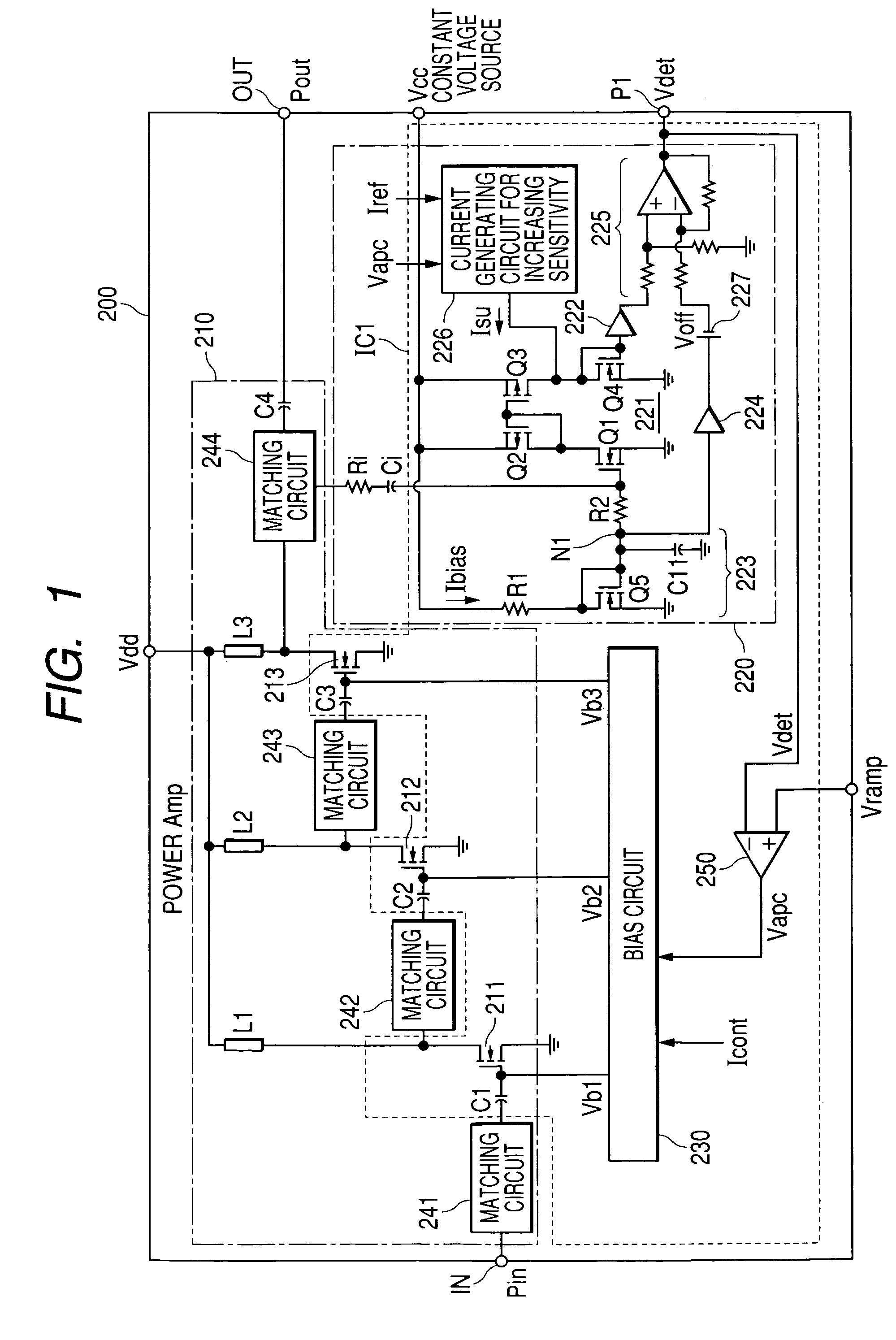
[0031]FIG. 1 shows an embodiment of a high frequency power amplifier (hereinbelow, called power module) to which an output power detection circuit of the invention is applied. In the specification, a structure constructed so as to be handled as a single electronic part by mounting a plurality of semiconductor chips and discrete parts on an insulating substrate such as a ceramic board on / in which print wiring is conducted and connecting the parts via the print wiring and bonding wires so that each part plays a predetermined role is called a module.

[0032]A power module 200 of the embodiment has a high frequency power amplifier 210 including a power amplification FET for amplifying an input high frequency signal Pin, an output power detection circuit 220 for detecting output power of the high frequency power amplifier 210, a bias circuit 230 for applying a bias voltage to the power amplification FET in each of stages of the high frequency power amplifier 210, thereby controlling idle c...

second embodiment

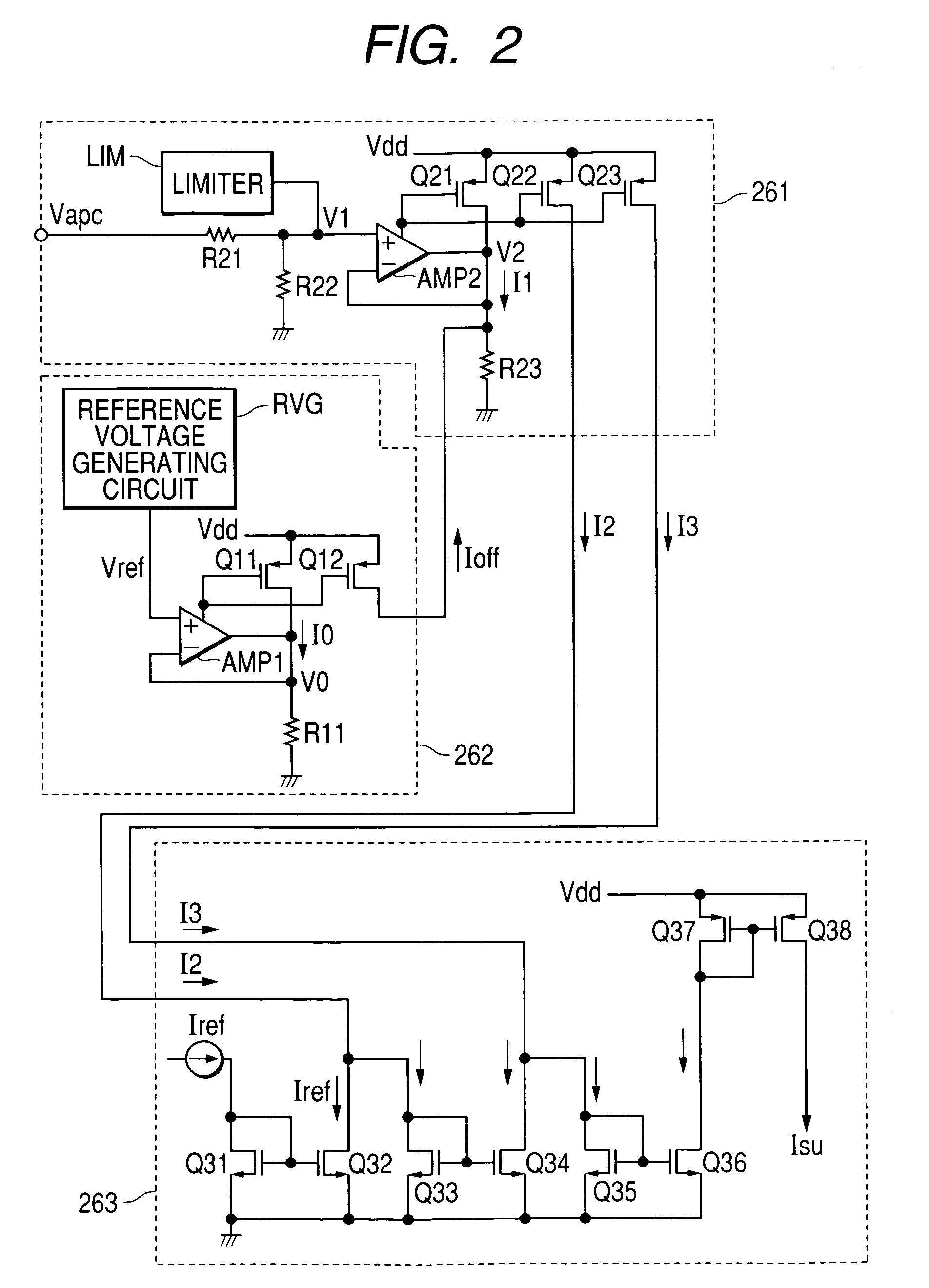
[0058]FIG. 7 shows a second embodiment of a power module to which the output power detection circuit of the invention is applied. In FIG. 7, the same reference numeral is designated to a circuit or device which is the same as that shown in FIGS. 1 and 2 and its description will not be repeated.

[0059]In the second embodiment, an operation point is given to the gate terminal of the transistor 213 for amplification in the final stage by a voltage obtained by dividing the output control voltage Vapc output from the error amplifier 250 by the resistors R31 and R32. Although not shown, an optimum operation point is given to each of the gate terminals of the transistors 211 and 212 for amplification in the first and second stages by a voltage obtained by dividing the output control voltage Vapc by the resistors at a different resistance ratio. In the second embodiment, the bias circuit 230 for applying the gate bias voltage of the transistors 211 to 213 for amplification is constructed by ...

example of application

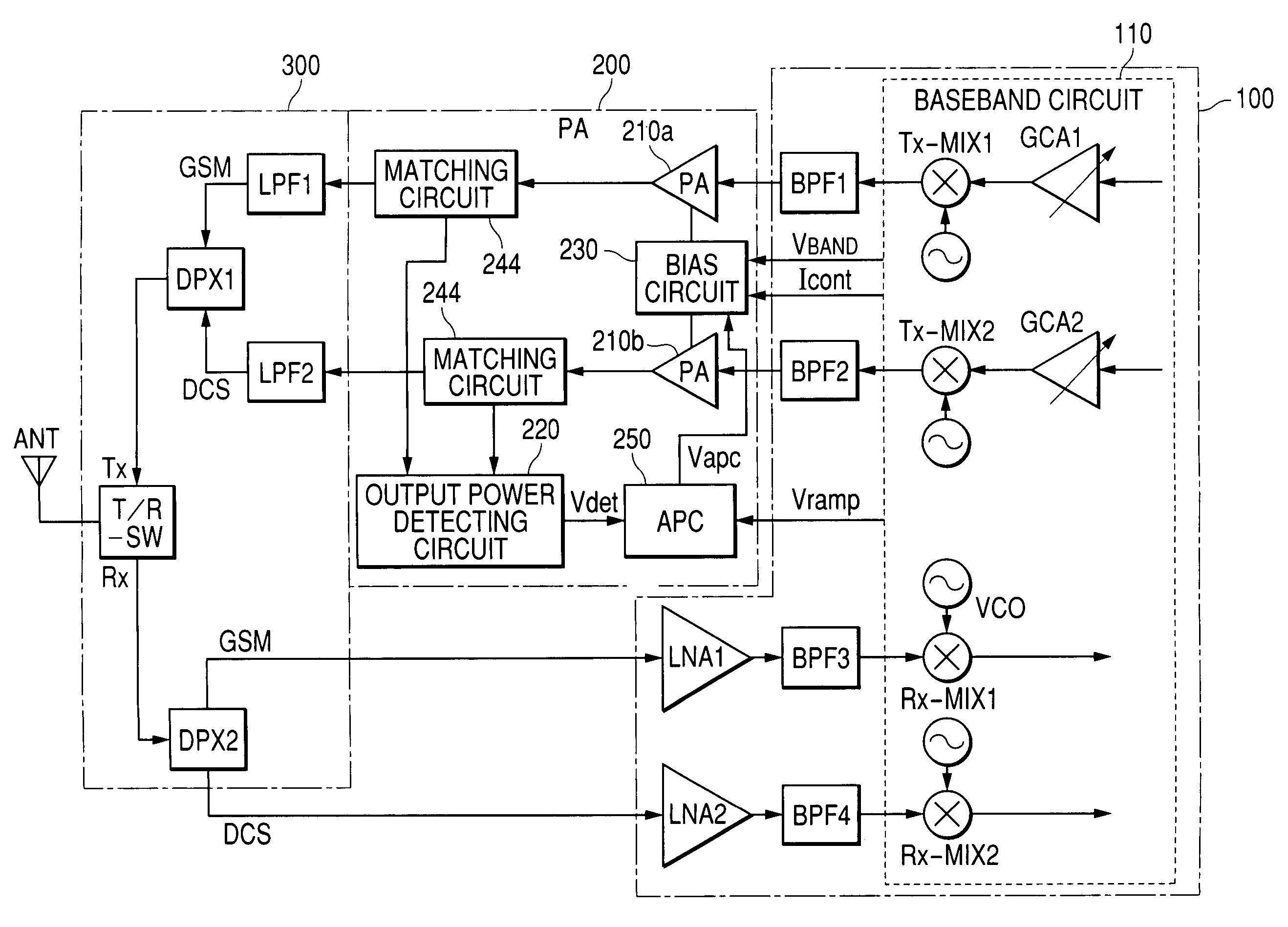
[0077]FIG. 12 shows a schematic configuration of a system capable of performing two radio communications in two communication systems of GSM and DCS as an example of a radio communication system which is effective when the power module of the embodiment is applied.

[0078]In FIG. 12, ANT denotes an antenna for transmitting / receiving signal electric waves, and 100 denotes an electronic device (hereinbelow, called an RF device) obtained by mounting, into a single package, a high frequency signal processing circuit (baseband circuit) 110 having a modulation / demodulation circuit capable of performing GMSK modulation and demodulation in the GSM and DCS systems and a circuit for generating I and Q signals on the basis of transmission data (baseband signal) and processing I and Q signals extracted from a reception signal, a semiconductor integrated circuit (baseband IC) for processing high frequency signals obtained by forming low noise amplifiers LNA1 and LNA2 for amplifying reception signa...


PUM


Abstract

The present invention provides a high frequency power amplifier circuit capable of obtaining sufficient detection output even in a range where a request output power level is low and performing a desired output power control by a control loop with the detection output in a radio communication system which detects output power and performs feedback control. An output power detection circuit which detects the level of output power on the basis of an AC signal supplied from a final amplification stage of a high frequency power amplification circuit via a capacitive element has a circuit configuration such that in a state where the output power control voltage is lower than a certain level, current (Isu) according to the output power control voltage is generated and supplied to the output power detection circuit, and detection sensitivity of the output power detection circuit improves according to the current.

Description

CROSS-REFERENCE TO RELATED APPLICATION[0001]The present application claims priority from Japanese patent application Nos. 2004-158689 filed on May 28, 2004 and 2004-000170 filed on Jan. 5, 2004, the content of which is hereby incorporated by reference into this application.BACKGROUND OF THE INVENTION[0002]The present invention relates to a technique effective when applied to an electronic part having a high frequency power amplifier circuit assembled therein, used for a radio communication system such as a mobile cellular phone and for amplifying a high frequency transmission signal and outputting the amplified signal, and more particularly, to a technique effective when used for a circuit for detecting output power necessary for an output power feedback control.[0003]Generally, in a transmission-side output part in a radio communication system (mobile communication system) such as a mobile cellular phone, a high frequency power amplifier circuit for amplifying a modulated transmiss...

Claims


Application Information

Patent Timeline
Patent Type & Authority Patents(United States)
IPC IPC(8): H04L25/03H03F3/24H03F3/193H03G3/30
CPCH03G3/3042H03G3/3047
Inventor SUGIYAMA, HIROKISOGA, TAKASHISHIMAMUNE, YUSUKETOMONO, SHUJIFURUYA, TOMIOTAKAHASHI, KYOICHI
Owner MURATA MFG CO LTD
Why Eureka
Try Eureka