Method for manufacturing a memory device having a nanocrystal charge storage region

a memory device and charge storage technology, applied in the field of memory devices, can solve the problems of degrading the charge storage capacity of the memory device, difficult to control the size distribution of the nanocrystal on the large diameter semiconductor wafer, and large variation in the size distribution of the nanocrystal

a memory device and charge storage technology, applied in the field of memory devices, can solve the problems of degrading the charge storage capacity of the memory device, difficult to control the size distribution of the nanocrystal on the large diameter semiconductor wafer, and large variation in the size distribution of the nanocrystal

US7335594B1Active Publication Date: 2008-02-26SPANSION LLC

Image

  • Method for manufacturing a memory device having a nanocrystal charge storage region
  • Method for manufacturing a memory device having a nanocrystal charge storage region
  • Method for manufacturing a memory device having a nanocrystal charge storage region

Examples


Embodiment Construction

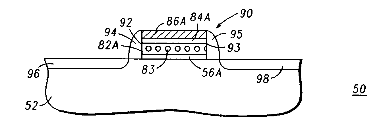
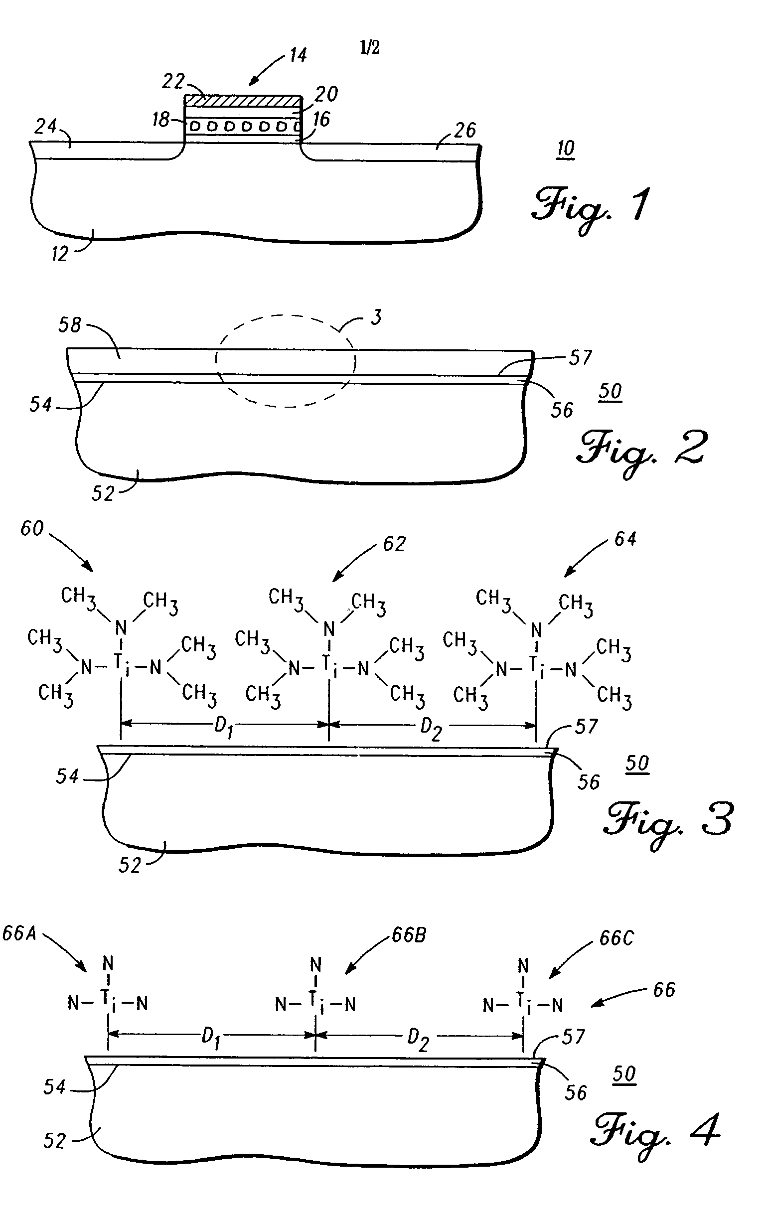
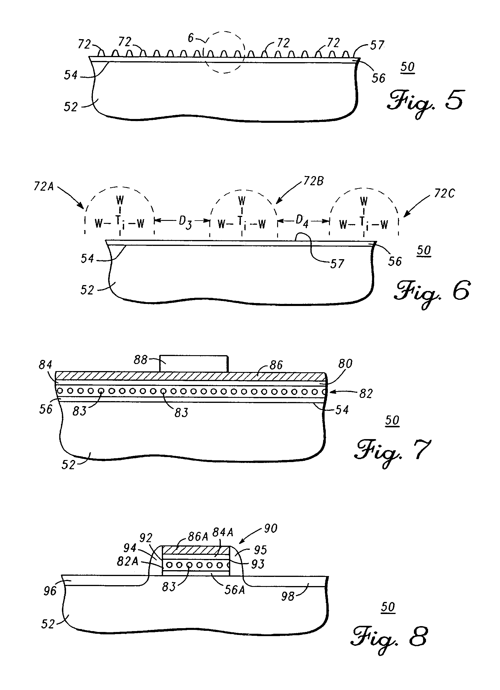
[0016]Generally, the present invention comprises a method for manufacturing a memory device having a nanocrystal charge storage region. In accordance with an embodiment of the present invention, precursor molecules bond to a dielectric substrate. The precursor molecules are comprised of a base structure or stem to which a plurality of ligands or constituent groups is bonded. The distance between adjacent base structures is governed by the size of the ligands. For example, when the precursor molecules are derived from tetrakis(dimethylamino)titanium (TDMAT), the base structure comprises a nitrogen atom bonded to a titanium atom and methyl ligands bonded to the nitrogen atom. The combination of the base structure and the methyl groups occupies a finite amount of space over the dielectric substrate and blocks other base structures and their associated methyl groups from occupying that same space. This phenomena is typically referred to as steric hindrance. The methyl groups are then st...


PUM


Abstract

A method for manufacturing a memory device having a metal nanocrystal charge storage structure. A substrate is provided and a first layer of dielectric material is grown on the substrate. An absorption layer is formed on the first layer of dielectric material. The absorption layer includes a plurality of titanium atoms bonded to the first layer of dielectric material, a nitrogen atom bonded to each titanium atom, and at least one ligand bonded to the nitrogen atom. The at least one ligand is removed from the nitrogen atoms to form nucleation centers. A metal such as tungsten is bonded to the nucleation centers to form metallic islands. A dielectric material is formed on the nucleation centers and annealed to form a nanocrystal layer. A control oxide is formed over the nanocrystal layer and a gate electrode is formed on the control oxide.

Description

FIELD OF THE INVENTION[0001]This invention relates, in general, to memory devices and, more particularly, to memory devices having metal nanocrystals in a charge storage region.BACKGROUND OF THE INVENTION[0002]As semiconductor device manufacturers shrink memory devices such as Flash memories and Dynamic Random Access Memories (DRAM's), the charge storage area in these devices decreases resulting in fewer stored electrons. One technique for increasing the number of stored electrons has been to incorporate nanocrystals in the charge storage region of a memory device. FIG. 1 illustrates a prior art memory device 10 having a layer of nanocrystal material disposed in the charge storage region. What is shown in FIG. 1 is a semiconductor substrate 12 on which a gate structure 14 is formed. Gate structure 14 includes a gate conductor 22 disposed on a dielectric stack comprising a tunnel oxide layer 16, a metal nanocrystal layer 18, and a control oxide layer 20. Source and drain regions 24 a...

Claims


Application Information

Patent Timeline
26 Feb 2008
Publication
US7335594B1
IPC
H01L21/44
CPC
B82Y10/00; H01L21/28273; H01L29/42332; H01L29/7881; H01L29/40114
Inventors
WANG, CONNIE PIN-CHIN; KRIVOKAPIC, ZORAN