

Chip package structure and chip packaging process
a chip and packaging technology, applied in the direction of electrical equipment, semiconductor devices, semiconductor/solid-state device details, etc., can solve the problems of chip packaging being more likely to warp or crack, the chip packaging is often miniaturized, and the thermal stress of non-uniform magnitude is often generated, so as to achieve the effect of significantly reducing the warping and cracking of the chip packag
- Summary
- Abstract
- Description
- Claims
- Application Information
AI Technical Summary
Benefits of technology
Problems solved by technology
Method used
Image

Examples
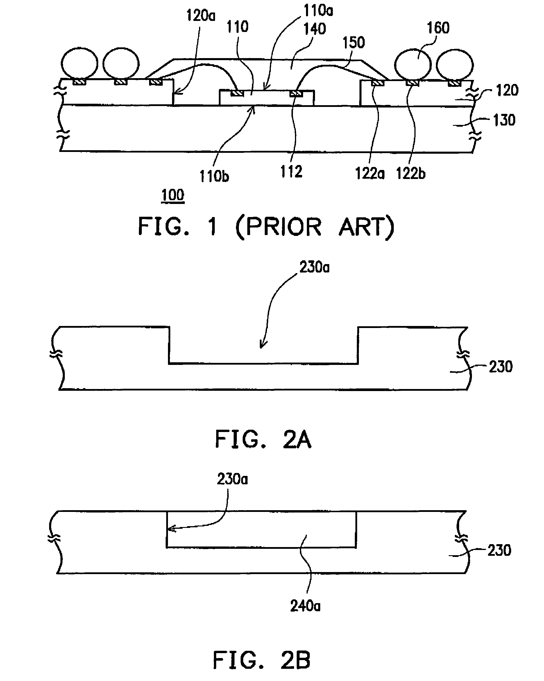
first embodiment
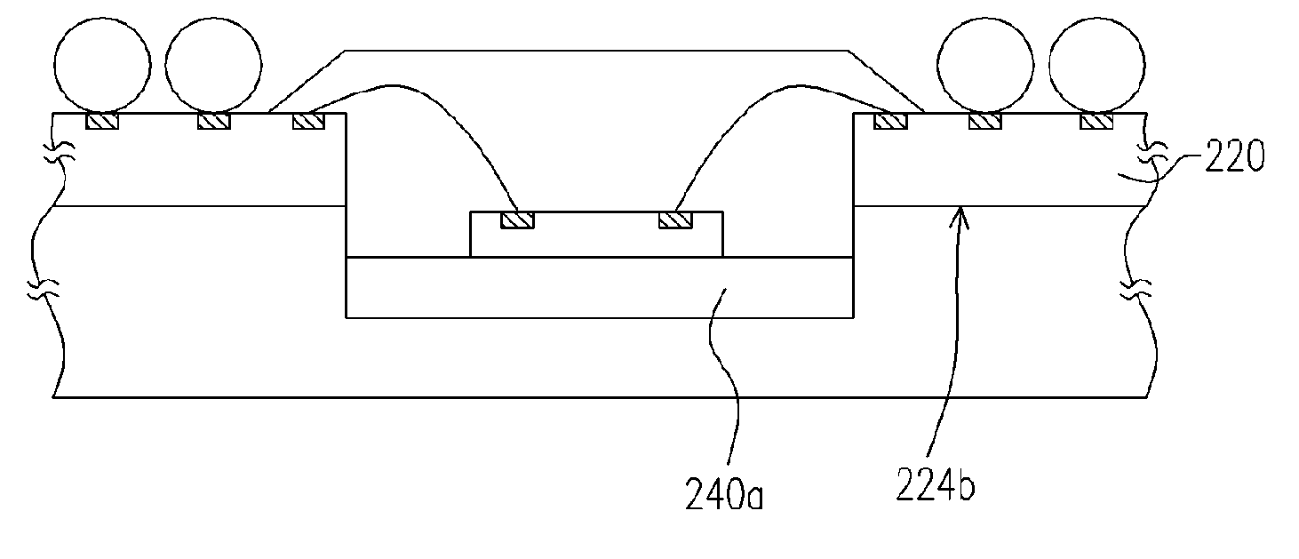
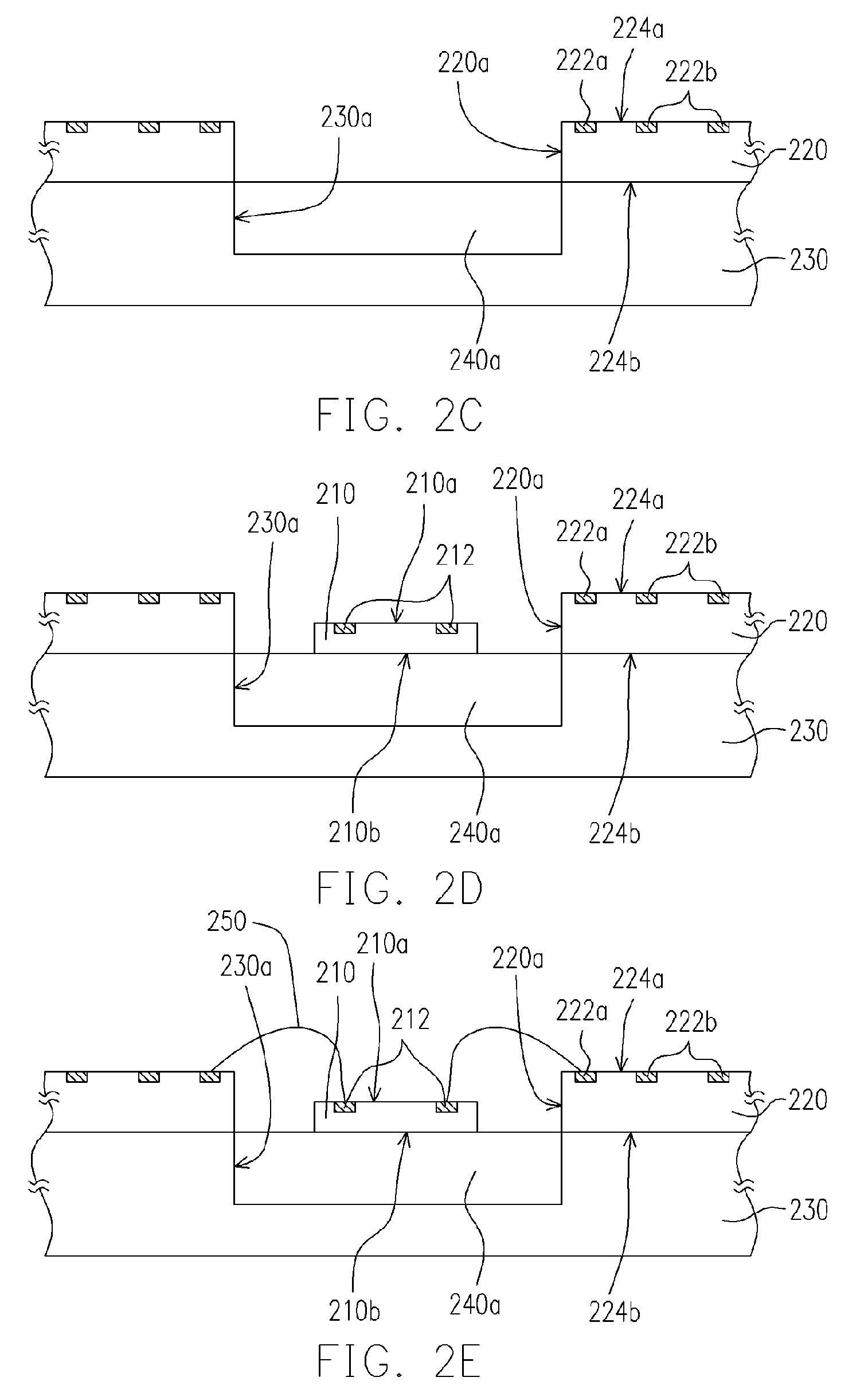
[0029]FIGS. 2A through 2G are schematic cross-sectional view showing the steps in a chip packaging process for producing a chip package according to the present invention. First, as shown in FIG. 2A, a cavity 230a is formed on a heat sink 230. The cavity 230a is formed, for example, by performing mechanical drilling, laser drilling or etching. As shown in FIG. 2B, a first encapsulant 240a is formed on the bottom of the cavity 230a by applying a material such as epoxy resin. Thereafter, as shown in FIG. 2C, a circuit substrate 220 is disposed on the heat sink 230. The circuit substrate 220 has an opening 220a that corresponds in position to the cavity 230a. Furthermore, the circuit substrate 220 has a top surface 224a having a plurality of first bonding pads 222a and a plurality of second bonding pads 222b thereon. The second bonding pads 222b are located around the first bonding pads 222a. The bottom surface 224b of the circuit substrate 220 is attached to the heat sink 230 by adhes...
second embodiment
[0034]Using the first type of chip package structure and its corresponding chip packaging process as a base, a chip package structure and chip packaging process having a higher heat dissipation can be produced. FIG. 5 is a schematic cross-sectional view of a first chip package structure according to the present invention. As shown in FIGS. 2G and 5, the chip package structure 300 in FIG. 5 has an additional heat-conductive interlayer 270 disposed between the chip 210 and the first encapsulant 240a. The heat-conductive interlayer 270 is fabricated by silver, copper or some other heat conductive metallic materials. Furthermore, the heat-dissipation layer 270 may extend between the circuit substrate 220 and the heat sink 230 so that heat generated by the chip 210 can be directly transferred to the heat sink 230 via the heat-conductive interlayer 270.
[0035]The chip packaging process for forming the chip package structure 300 in FIG. 5 includes performing an electroplating to form the he...
PUM
 Abstract
Description
Claims
Application Information