Printed wiring board with enhanced structural integrity

a technology of structural integrity and printed wiring, applied in the field of printed wiring boards, can solve the problems of high parts count, increased documentation, procurement and logistic difficulties, and often required manual labor for assembling these panels and electronics, and achieve the effect of enhancing structural performan

Active Publication Date: 2008-03-11
HARRIS CORP
View PDF14 Cites 12 Cited by
  • Summary
  • Abstract
  • Description
  • Claims
  • Application Information

AI Technical Summary

Benefits of technology

[0006]It is therefore an object of the present invention to provide a structural printed wiring board panel that can be used in a circuit card assembly that incorporates all electrical functions and provides enhanced structural performance, overcoming the disadvantages of the prior art indicated above.
[0007]The present invention is a large structural printed wiring board that incorporates all the electrical functions of smaller, less rigid prior art printed wiring boards used in circuit card assemblies. In one aspect of the present invention, an external metallic skin or face sheet is secured, such as by adhesive lamination, to each face of a multilayer printed wiring board (although only one face is possible) for enhanced structural performance. The face sheet also is operative as a ground plane layer. This provides excellent structural properties because the face sheets contribute high stiffness at outer bending fibers forming a board. The face sheets also spread heat, providing superior thermal performance. Because the face sheets carry substantial structural load, the overall printed wiring board has a lower weight when RF components and patch antenna elements are added, forming the circuit card assembly.
[0008]With the present invention, standard printed wiring board facilities and manufacturing processes can be used to build a single printed wiring board to replace the use of many printed wiring boards. Selective plating can be used for component mounting and interconnects. Plating can also be used to electrically connect the face sheets to any underlying printed wiring board and provide good RF ground plane functionality and enhanced heat transfer.
[0009]In accordance with the present invention, a structural printed wiring board (PWB) panel of the present invention includes a multilayer printed wiring board having opposing outer faces and interlayer interconnects that route RF, power and control signals. The interlayer interconnects can be surface interconnects. Connection areas are formed on at least one face for connecting interlayer interconnects and any electrical components of the multilayer printed wiring board. A metallic face sheet is secured onto at least one opposing outer face, adding structural rigidity to the multilayer printed wiring board. In one aspect of the present invention, each opposing outer face includes a face sheet. Each face sheet has apertures that are formed to allow access to connection areas from electrical components, such as RF components or antenna elements, mounted on the face sheets.

Problems solved by technology

Manufacturing very large surface area boards associated with phased array antenna arrays provides several challenges.
Manual labor often is required for assembling these panels and electronics, typically using screws or similar fasteners.
Extensive interconnects integrate different boards, often requiring a high parts count, adding to the documentation, procurement and logistic difficulties associated with the development, manufacture and sale of such boards.
Antenna elements and feed networks also require complex grounding.
These boards overall only have a modest weight efficiency.
Some of these approaches still maintain a low structural integrity, however.
These proposals often produce circuit card assemblies having limited environmental robustness and mandate a larger number of mounting points per card to secure the card to a housing or other support structure.
These proposals also have a low weight efficiency and use surface mounted discrete components and radio frequency (RF) “modules.”
For example, some metallic heat sinks are laminated to printed wiring boards, but this assembly process does not provide intimate electrical contact even if accomplished with electrically conductive adhesives.
Some conductive adhesives have a low shear efficiency and yield assemblies with poor stiffness and strength.
Some printed wiring boards have copper metallic layers, but these layers have contributed little to the printed wiring board structure because of their limited thickness and low specific stiffness in design.
Other boards have poor coefficient of thermal expansion (CTE) with devices and / or other board materials forming the overall circuit card assembly.

Method used


Image

  • Printed wiring board with enhanced structural integrity
  • Printed wiring board with enhanced structural integrity
  • Printed wiring board with enhanced structural integrity

Examples


Embodiment Construction

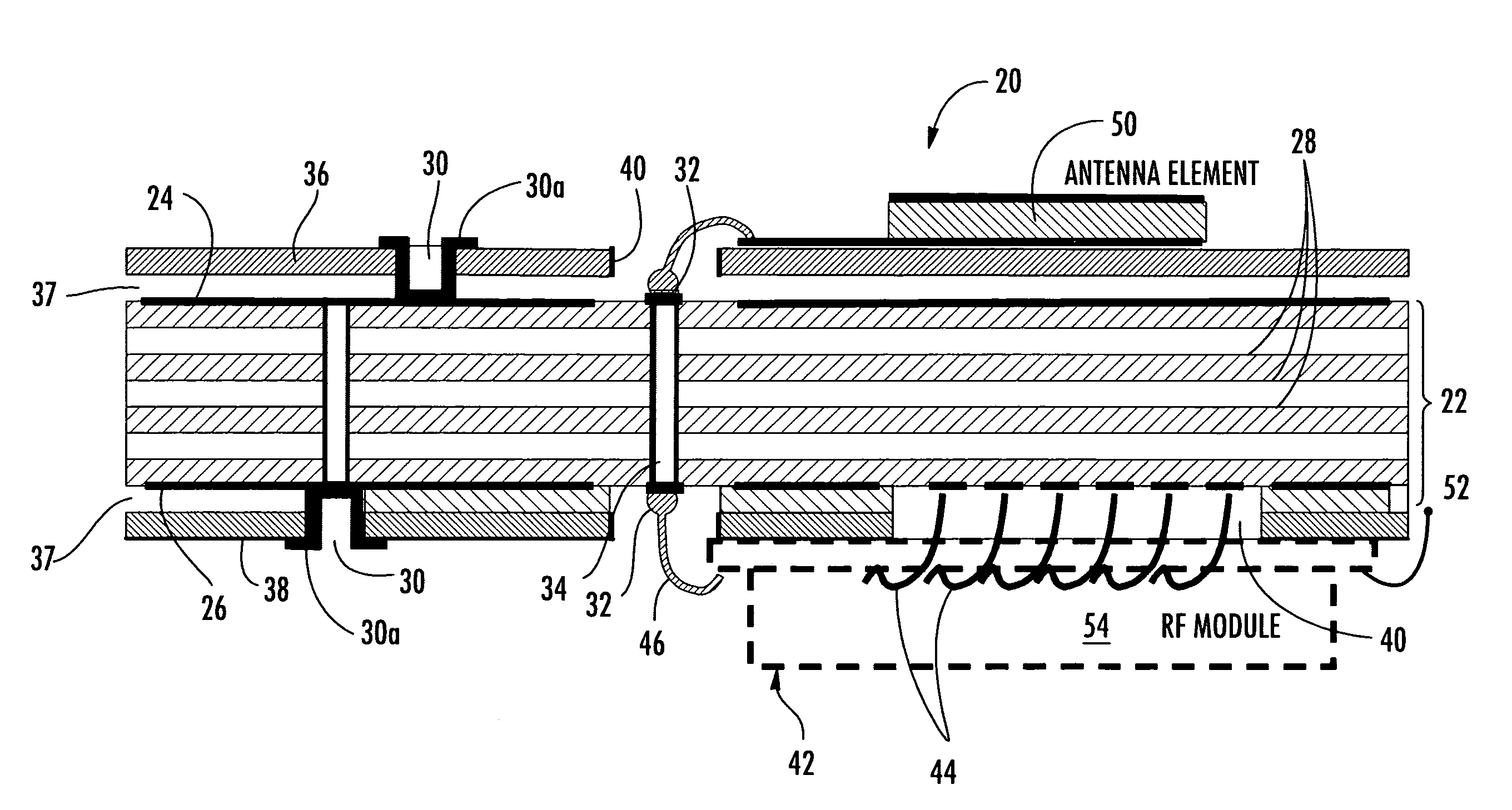
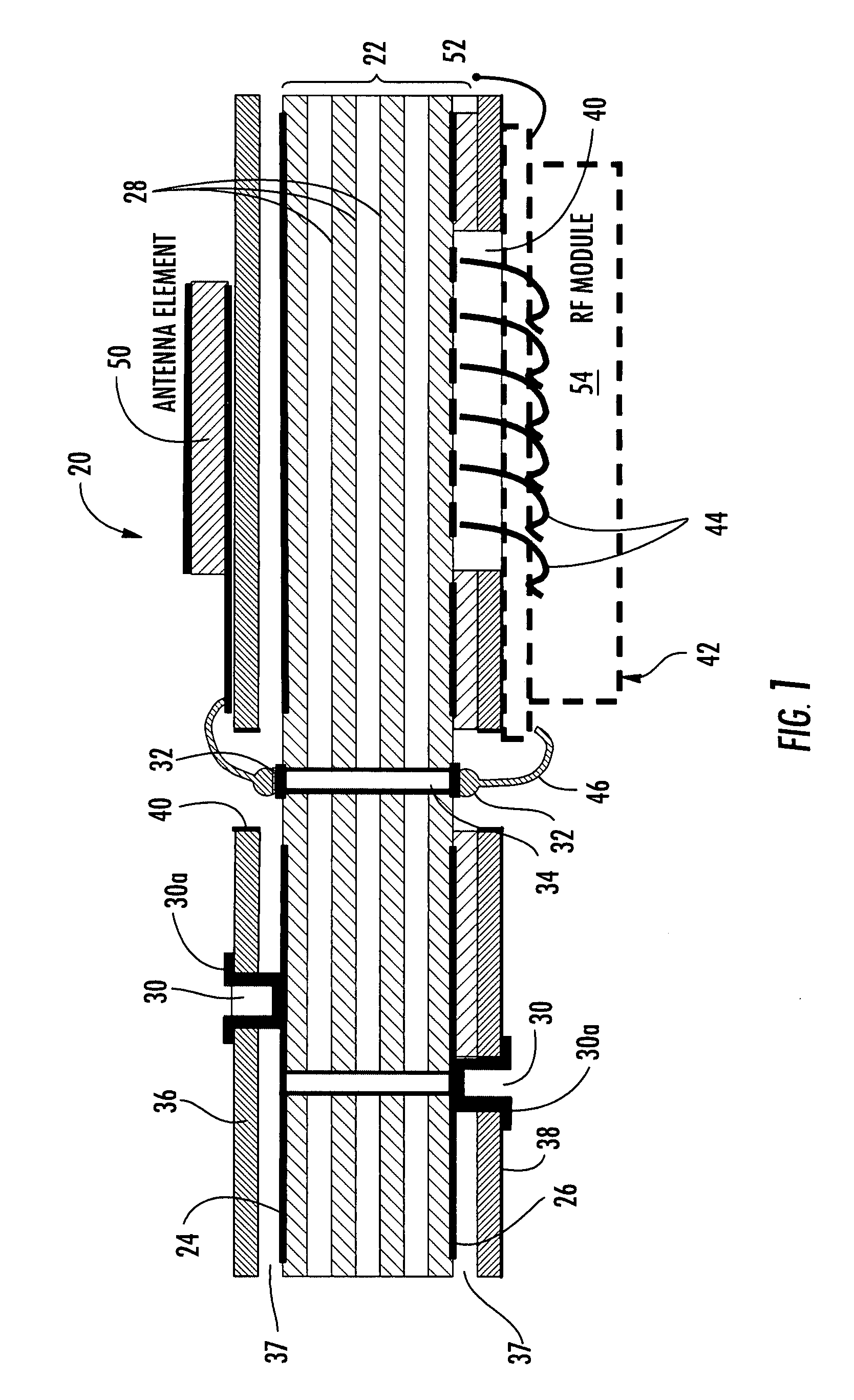
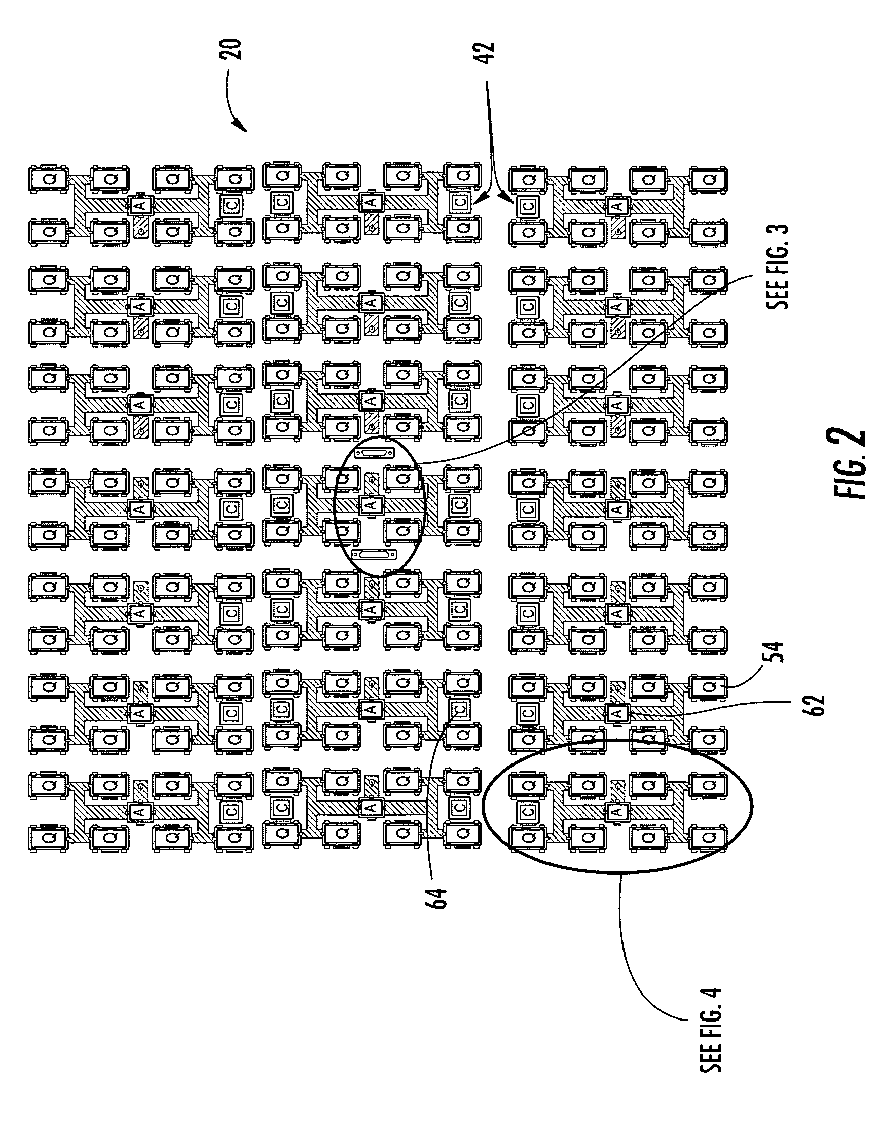
[0030]The present invention will now be described more fully hereinafter with reference to the accompanying drawings, in which preferred embodiments of the invention are shown. This invention may, however, be embodied in many different forms and should not be construed as limited to the embodiments set forth herein. Rather, these embodiments are provided so that this disclosure will be thorough and complete, and will fully convey the scope of the invention to those skilled in the art. Like numbers refer to like elements throughout, and prime notation is used to indicate similar elements in alternative embodiments.

[0031]The present invention is a large structural printed wiring board that incorporates all the electrical functions of smaller, less rigid prior art printed wiring boards, which include various electrical components, forming circuit card assemblies. The present invention uses an external metallic skin or face sheet secured, such as by adhesive lamination, to each side or ...


PUM

PropertyMeasurementUnit
thickaaaaaaaaaa
thickaaaaaaaaaa
structural rigidityaaaaaaaaaa

Abstract

A structural printed wiring board panel includes a multilayer printed wiring board having opposing, outer faces and interlayer interconnects that route RF, power and control signals. Connection areas are formed in or on at least on one face for connecting the interlayer interconnects and any electrical components. A metallic face sheet is secured onto at least one outer face, adding structural rigidity to the multilayer printed wiring board. A metallic face sheet can have apertures positioned to allow access to connection areas. RF components can be carried by a face sheet and operatively connected to connection areas. Antenna elements can be positioned on the same or an opposing face sheet and operatively connected to RF components to form a phased array printed wiring board (PWB) panel.

Description

FIELD OF THE INVENTION[0001]The present invention relates to the field of printed wiring boards, and more particularly, this invention relates to a printed wiring board (PWB) panel that has enhanced structural integrity.BACKGROUND OF THE INVENTION[0002]Lightweight, low cost printed wiring board panels used in planar or conformal phased array avionic applications, high speed digital boards, and power distribution boards, for example, require easy interconnect, continuous ground planes and optimized thermal and structural performance. Manufacturing very large surface area boards associated with phased array antenna arrays provides several challenges. For example, the radio frequency, control and power signals must be distributed over a large area. Array or other different self-supporting panels must provide low weight per unit area and be manufactured and assembled in an efficient manner without undue interconnect complexity.[0003]Some prior art printed wiring boards are formed as cir...

Claims


Application Information

Patent Timeline
Patent Type & Authority Patents(United States)
IPC IPC(8): H05K7/02H05K7/06H05K7/08H05K7/10H01Q3/26H01Q21/00H05K1/02H05K1/09H05K3/42
CPCH01Q3/26H01Q21/0006H01Q21/0037H05K1/0243H05K3/429Y10T29/49165H05K2201/09509H05K2201/09554H05K2201/0959H05K2201/10553H05K2203/049H05K2201/0347H01Q21/065
Inventor JANDZIO, GREGORY M.PEDERSEN, ANDERS P.RIEF, GARY A.WHYBREW, WALTER M.
Owner HARRIS CORP
Why Eureka
Try Eureka