Complementary nonvolatile memory device

a non-volatile, memory technology, applied in semiconductor devices, digital storage, instruments, etc., can solve the problems of significant power dissipation, increase in operating resistance, and relatively slow reading speed, so as to improve operating speed, overcome the limitation of bit scale-up, and improve the effect of reading speed

Active Publication Date: 2008-03-18
SAMSUNG ELECTRONICS CO LTD
View PDF2 Cites 21 Cited by
  • Summary
  • Abstract
  • Description
  • Claims
  • Application Information

AI Technical Summary

Benefits of technology

[0012]It is a feature of an embodiment of the present invention to provide a complementary nonvolatile memory device that increases the number of bits per cell.
[0085]After the data state of any one of the nonvolatile PMOS and NMOS memories may be read, the data state of the other may be read using a curve showing a complementary relationship therebetween. Thus, a read operation may be shortened. Write and erase operations may be performed in cell units, rather than in block units, which may improve operating speed and reduce power dissipation.

Problems solved by technology

However, reading speed may be relatively slow, since a pertinent block must be selected before being read and serial connection of cells leads to an increase in operating resistance.
Also, since the conventional flash memory operates in such a manner that previous data may be entirely erased and new data may be rewritten irrespective of previous memory state, resulting in significant power dissipation.
If the number of bits per cell is two or more, a current difference measured at the reading voltage may be high and a large current may be supplied, thus dissipating a large amount of power.
Thus, a continuous bit scale-up may be difficult.
However, this method is a current detecting method and typically requires complicated circuit construction including comparators and sense amplifiers.

Method used


Image

  • Complementary nonvolatile memory device
  • Complementary nonvolatile memory device
  • Complementary nonvolatile memory device

Examples


embodiment 1

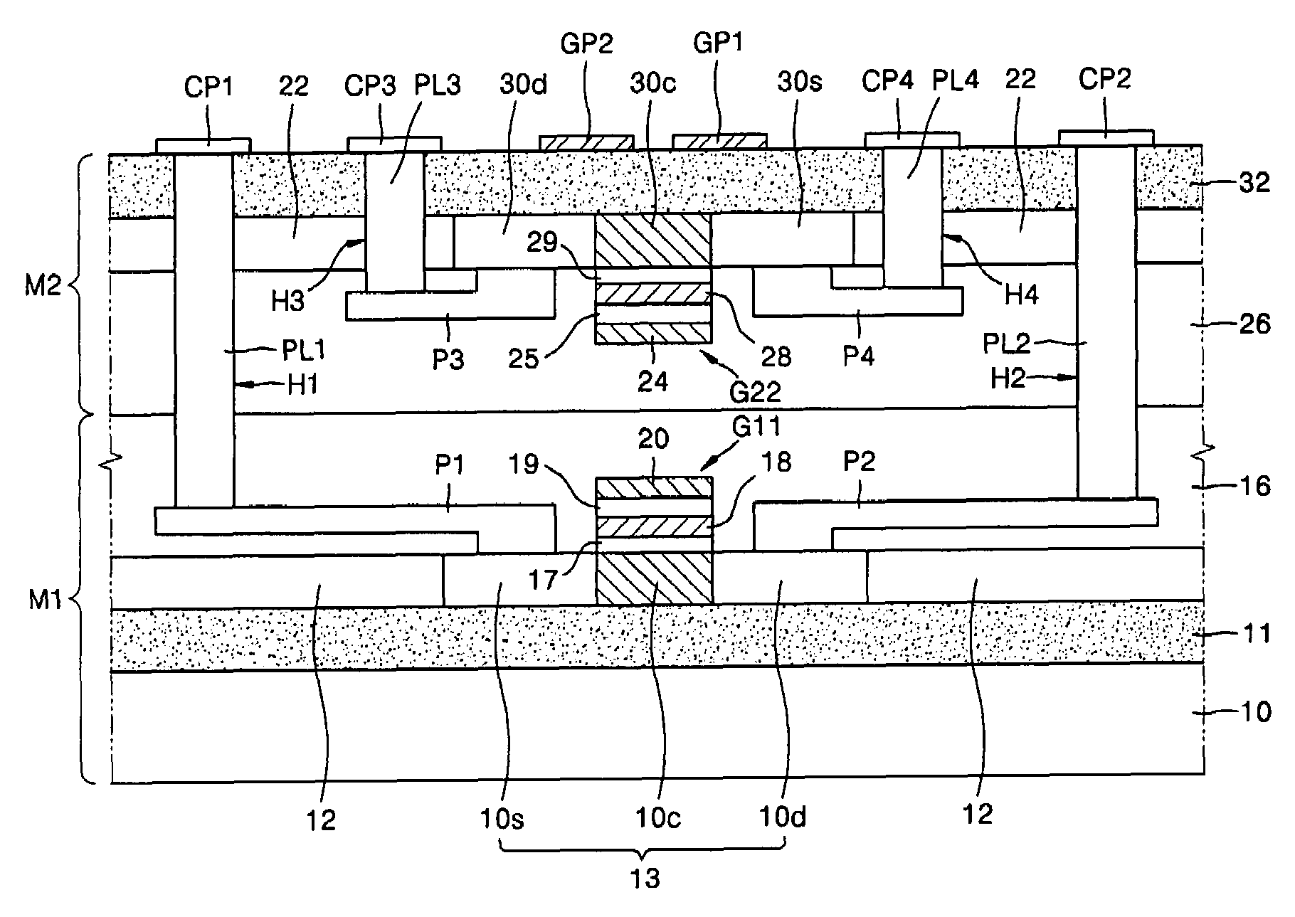
[0117]Referring to FIG. 1, a first memory device may include a first nonvolatile memory M1 and a second nonvolatile memory M2, which is vertically and sequentially stacked. The first and second nonvolatile memories M1 and M2 are secured together. The first and second nonvolatile memories M1 and M2 may include a storage unit for storing multi-bit data in a gate stacked structure. The first and second nonvolatile memories M1 and M2 may be a P-type transistor and an N-type transistor, e.g., a P-type SONOS memory and an N-type SONOS memory, respectively, each of which can store data and function as a switch.

[0118]The first nonvolatile memory M1 may include a first substrate 10 and an insulating layer 11 disposed on the first substrate 10. Shallow trench isolation (STI) layers 12 may be disposed on the insulating layer 11 and separated from each other. A semiconductor substrate 13 may be disposed on the insulating layer 11 between the STI layers 12. The semiconductor substrate 13 may inc...

embodiment 2

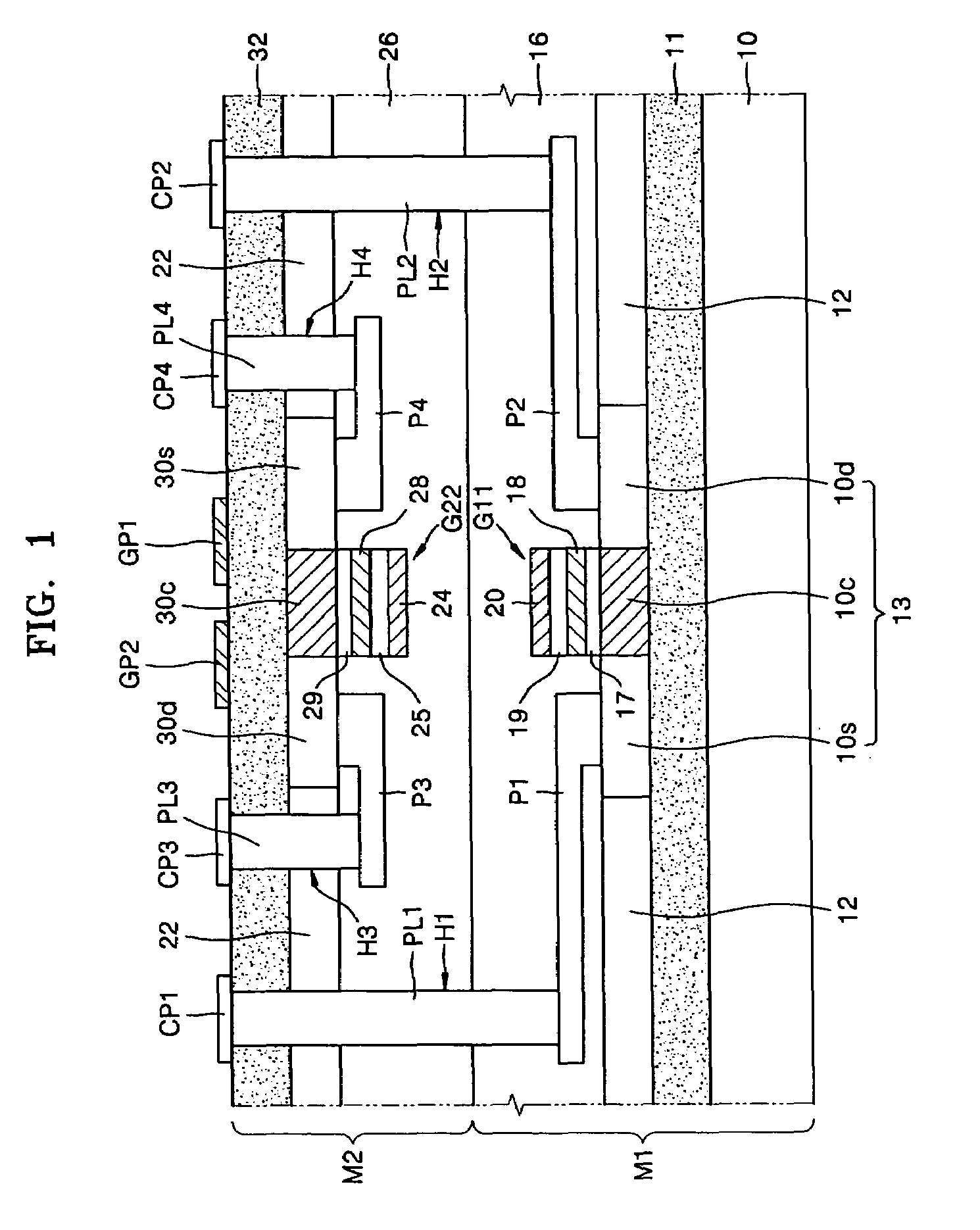
[0128]A nonvolatile memory device according to a second embodiment of the present invention (hereinafter, referred to as a “second memory device”) may be different from the first memory device in that it includes a second nonvolatile memory M22 instead of the second nonvolatile memory M2. In the second nonvolatile memory M22, the same reference numerals are used to denote the same elements as in the second nonvolatile memory M2. Also, since a first nonvolatile memory M1 of the second memory device may be the same as that of the first memory device, a detailed illustration thereof may be omitted in FIG. 2.

[0129]Referring to FIG. 2, the second nonvolatile memory M22 may include the insulating layer 32, the semiconductor substrate (not shown) disposed on the insulating layer 32, and the second gate stacked structure G22 disposed on the semiconductor substrate. The semiconductor substrate may be surrounded by the STI layer 22. The semiconductor substrate may include the first impurity r...

embodiment 3

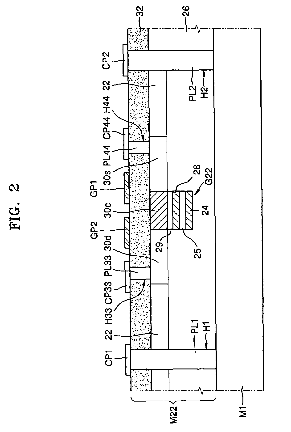
[0130]Referring to FIG. 3, a nonvolatile memory device according to a third embodiment of the present invention (hereinafter, referred to as a “third memory device”) may include a first nonvolatile memory M11 and a second nonvolatile memory M222, which may be sequentially stacked. The first and second nonvolatile memories M11 and M222 may be bonded to each other.

[0131]A first contact pad layer P11 and a second contact pad layer P22 of the first nonvolatile memory M11 may have different shapes from the first and second contact pad layers P1 and P2 of the first nonvolatile memory M1 of the first memory device shown in FIG. 1. Likewise, a third contact pad layer P33 and a fourth contact pad layer P44 of the second nonvolatile memory M222 may have different shapes from the third and fourth contact pad layers P3 and P4 of the second nonvolatile memory M2 of the first memory device.

[0132]Specifically, while the first and second contact pad layers P1 and P2 of the first nonvolatile memory ...


PUM


Abstract

Provided are a complementary nonvolatile memory device, methods of operating and manufacturing the same, a logic device and semiconductor device having the same, and a reading circuit for the same. The complementary nonvolatile memory device includes a first nonvolatile memory and a second nonvolatile memory which are sequentially stacked and have a complementary relationship. The first and second nonvolatile memories are arranged so that upper surfaces thereof are contiguous.

Description

BACKGROUND OF THE INVENTION[0001]1. Field of the Invention[0002]The present invention relates to a memory device, and a method of manufacturing the same. More particularly, the present invention relates to a complementary nonvolatile memory device, methods of operating and manufacturing the same, a logic device and semiconductor device including the same, and a reading circuit for the same.[0003]2. Description of the Related Art[0004]Nonvolatile memory devices include read only memory (ROM), which can be categorized as a mask ROM, which is programmed during manufacture, an electrically erasable and programmable read only memory (EEPROM), and others. A flash memory, which is also a nonvolatile memory device, is a modification of a conventional EEPROM, and includes a cell array in which erasing is performed in block units, sector units, or chip units and programming is performed in bit units.[0005]The architecture of a flash memory can be divided into a NOR type and a NAND type. Cells...

Claims


Application Information

Patent Timeline
Patent Type & Authority Patents(United States)
IPC IPC(8): G11C5/06G11C11/56G11C16/04G11C16/28H01L21/8247H01L27/06H01L27/115
CPCG11C11/5621H01L27/0688H01L27/11521H01L27/11551H10B41/20H10B41/30
Inventor PARK, YOON-DONGLEE, JO-WONKIM, CHUNG-WOOLEE, EUN-HONGSEO, SUN-AEKIM, WOO-JOOCHAE, HEE-SOONCHAE, SOO-DOOSONG, I-HUN
Owner SAMSUNG ELECTRONICS CO LTD
Why Eureka
Try Eureka