Method for estimating propagation noise based on effective capacitance in an integrated circuit chip

a technology of effective capacitance and propagation noise, applied in the direction of instruments, computing, electric digital data processing, etc., can solve the problems of increasing noise in digital integrated circuits (ics), difficult to model the non-linear behavior of gates using a simple linear model, and usually impractically slow to directly analyze the global signal net. achieve the effect of improving the accuracy of existing noise analysis tools

Inactive Publication Date: 2008-03-18
GOOGLE LLC
View PDF7 Cites 19 Cited by
  • Summary
  • Abstract
  • Description
  • Claims
  • Application Information

AI Technical Summary

Benefits of technology

[0009]Accordingly, it is an object of the invention to improve the accuracy of existing noise analysis tools in order to identify wires susceptible to noise problems such that other tools can solve the noise problems in the design.
[0010]It is another object of the invention to minimize the increase in run time of the noise analysis tool while executing a more accurate analysis.
[0011]It is yet another object of the invention to improve and accurately predict signal integrity issues in high performance digital integrated circuits.
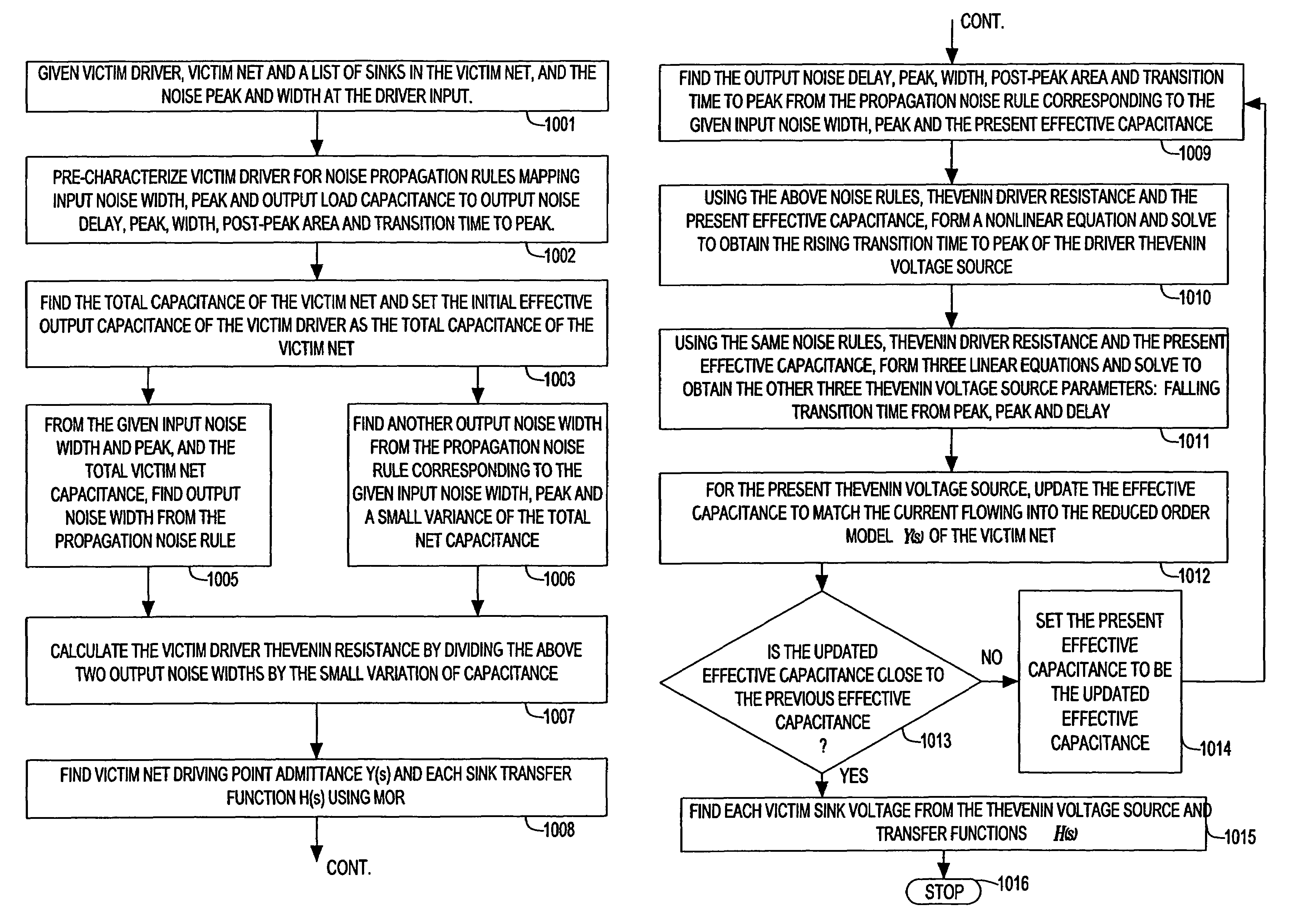
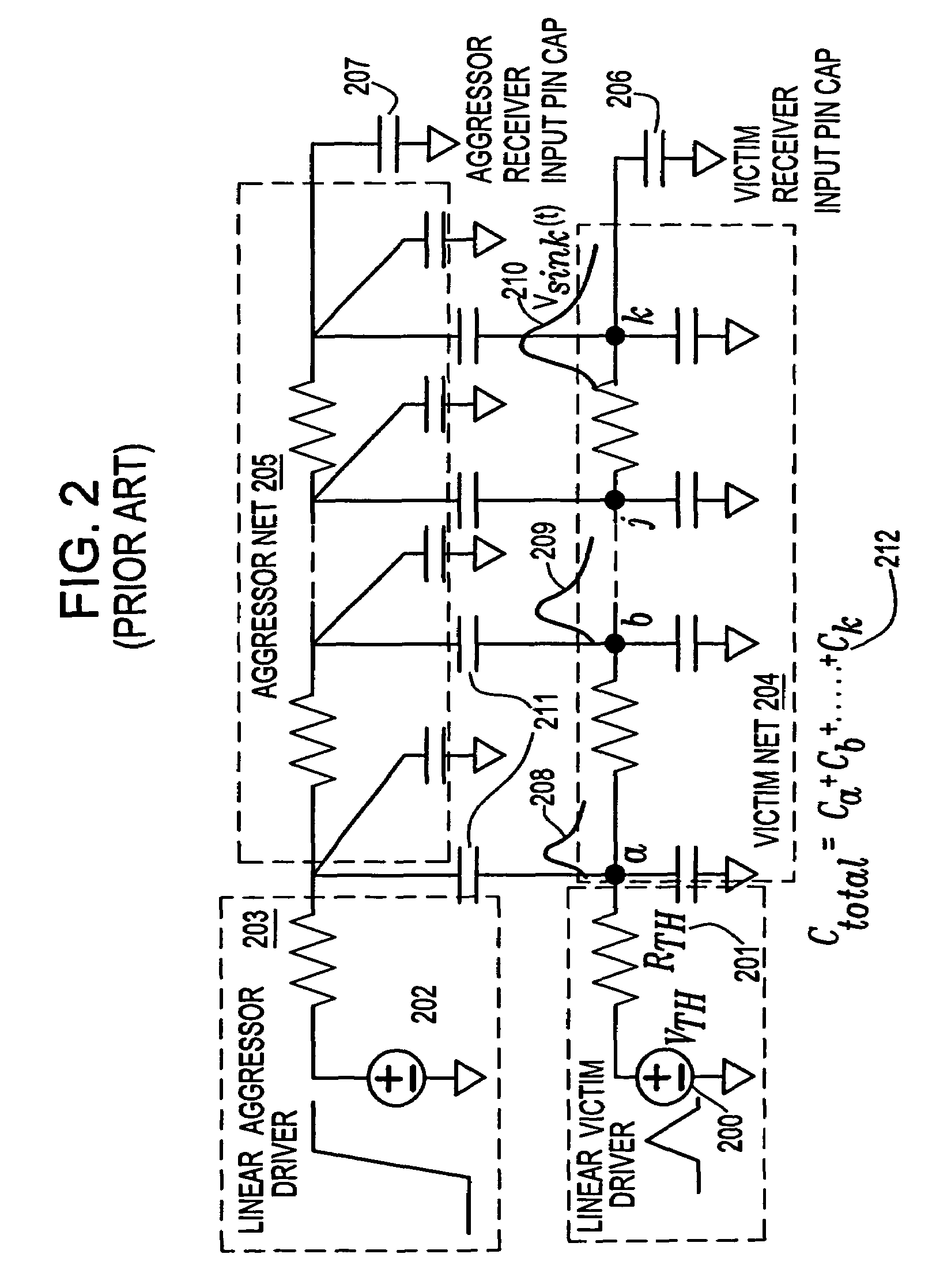
[0013]The present invention provides further a noise-driven effective capacitance solution for estimating propagation noise induced by a non-zero noise glitch at the input of the driving gate. Gate propagation noise rules describing a relationship between the output noise properties and the input noise properties and the output loading capacitance are used within the noise-driven effective capacitance process to determine the linear Thevenin model of the driving gate. The noise rules are either pre-characterized as a look-up table using SPICE or analyzed using a simple non-linear behavioral model of the gate. The linearized Thevenin driver model is then employed to analyze both the propagation noise and the combined coupling and propagation noise typically seen in global signal nets. The present invention extends a conventional timing driven effective capacitance method into the noise domain. Similar to the effective capacitance method in timing analysis which is widely used in industry timing tools, this approach provides a successful mechanism for separating the non-linear driver analysis from the linear interconnect analysis. In addition, the linear driver model maintains the linear property of the overall circuit, upon which superposition is applied to ease the task of finding the peak alignment of all the propagation and coupling noise sources.
[0015]The propagation noise in an interconnect is computed by convolving the Thevenin voltage source with the transfer function of the linear interconnect circuit. The same Thevenin model is employed to analyze propagation noise in the presence of coupling noise caused by the simultaneous switching of aggressor nets capacitively or inductively coupled to the victim net. The coupling and propagation noise peak alignment is trivially achieved by superposition. This approach works both accurately and efficiently for estimating the propagation noise and the combined propagation and coupling noise.
[0016]Additionally, the present invention provides a method for minimizing noise problems in a chip design, the chip design including at least one driver gate driving a victim net and sinks attached to the victim net, the method including the steps of: a) identifying noise at the inputs of the driver gate and computing the noise at the output thereof; b) propagating the computed noise at the output to all the sinks attached to the victim net; c) identifying nets coupled to the victim net and signal transitions on thecoupled nets, and computing the coupled noise for all the sinks attached to thevictim net; d) adding the computed propagation noise to the computed coupled noise; e) iteratively repeating steps a) to d) until a latch is reached; and f) determining if the noise at the latch input overlaps a signal clock, the overlap being indicative of a chip failure.

Problems solved by technology

The continuous scaling of CMOS processes has lead to an increase of noise in digital integrated circuits (ICs).
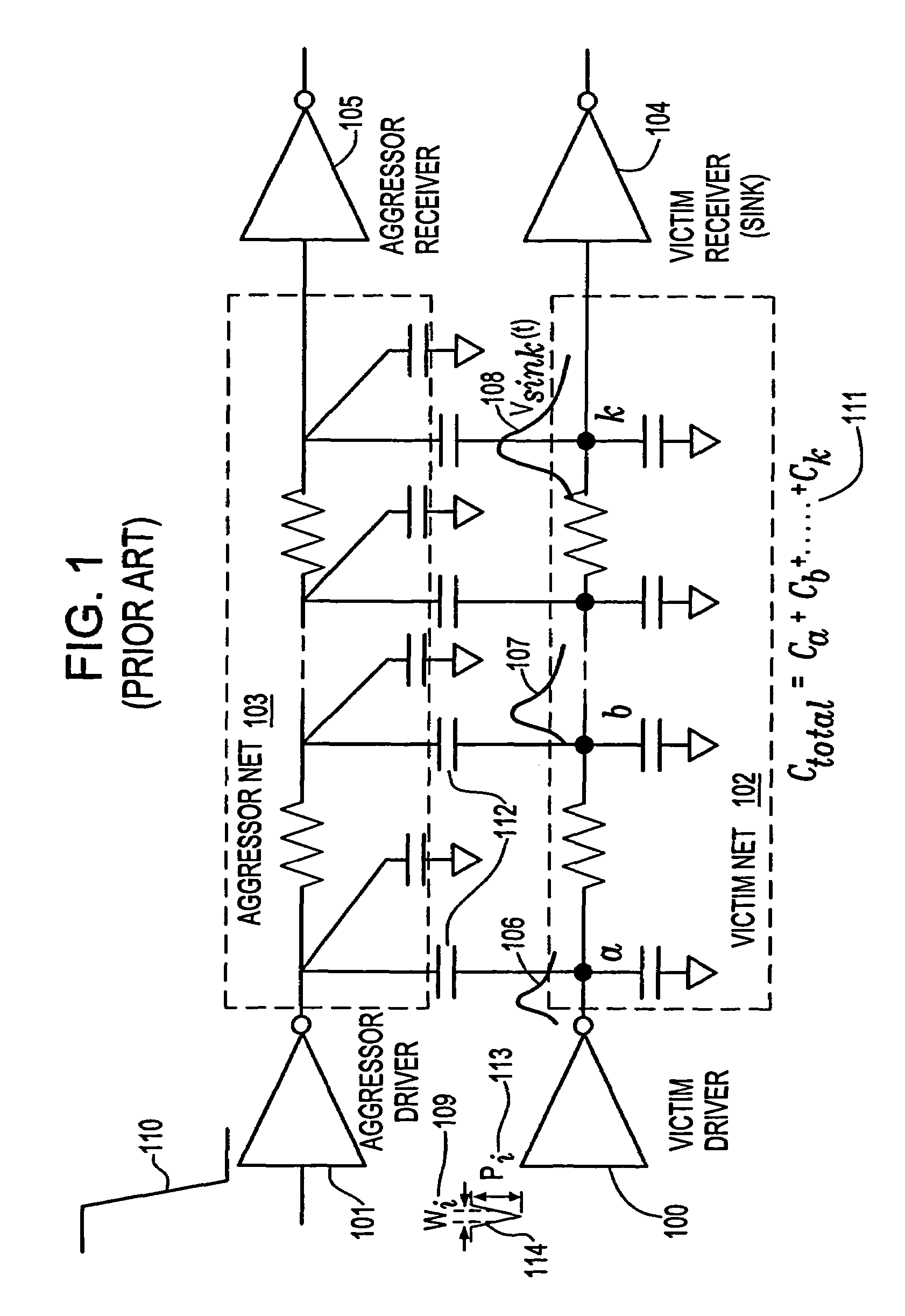
It is usually impractically slow to directly analyze the global signal net shown in FIG. 1 using a non-linear circuit analyzer.
However, it is rather challenging to model the non-linear behavior of a gate using a simple linear model.
Such an approach typically introduces a considerable amount of error.
One limitation of such a behavioral model is that it works well only for single stage gates.
Moreover, the introduction of the non-linear model in the circuit makes the worst-case peak alignment between the victim and aggressors costly.
However, this approach raises concerns in the computational cost of the model parameters.

Method used


Image

  • Method for estimating propagation noise based on effective capacitance in an integrated circuit chip
  • Method for estimating propagation noise based on effective capacitance in an integrated circuit chip
  • Method for estimating propagation noise based on effective capacitance in an integrated circuit chip

Examples


example

[0115]Referring now to FIG. 10, a circuit typicaly found in a digital VLSI chip is shown and will be used to illustrate various aspects of the invention.

[0116]L1 and L2 are latches and G1, G2, and G3 are combinational logic gates. RLC wires N1, N2, N3, and N4 interconnect the latches and the gates with each other. L1 is clocked by clock C1, and L2 by clock C2. The clocking scheme is shown to the right of the figure. Data is launched from latch L1 at the edge E1 of C1, and after passing through gate G1, it is captured by latch L2 at clock edge E3 of C2. Simultaneously, the data after passing through G2 and G3 is captured by latch L1 at the edge E2 of C1. Also shown, are wires that run adjacent to N1, N2 and N4 denoted by P1, P2, P3 and P4, respectively. These adjacent wires have both capacitive and inductive coupling to N1, N2 and N4. Therefore, any signal transitions on these adjacent wires induce noise which interferes with the data launched by L1, forcing incorrect data to be capt...


PUM


Abstract

A system and method for estimating propagation noise that is induced by a non-zero noise glitch at the input of the driver circuit. Such propagation noise is a function of both the input noise glitch and the driver output effective capacitive load, which is typically part of the total wiring capacitance due to resistive shielding in deep sub-micron interconnects. The noise-driven effective capacitance solution provided herein also estimates the propagation noise induced by a non-zero noise glitch at the input of the driving gate. Gate propagation noise rules describing a relationship between the output noise properties and the input noise properties and the output loading capacitance are used within the noise-driven effective capacitance process to determine the linear Thevenin model of the driving gate. The linearized Thevenin driver model is then employed to analyze both the propagation noise and the combined coupling and propagation noise typically seen in global signal nets.

Description

BACKGROUND OF THE INVENTION[0001]The present invention relates to the design of integrated circuit chips, and more particuarly, to a method and a system for improving the accuracy of existing noise analysis tools in order to identify wires susceptible to noise problems such that other tools can resolve the noise problems in the design.[0002]The continuous scaling of CMOS processes has lead to an increase of noise in digital integrated circuits (ICs). Noise glitches that propagate to a dynamic node or storage element (e.g., a latch) can alter the state of the circuit. This type of noise is often called functional noise. There are two types of noise glitches in a victim net. The first one is coupling noise, which refers to the noise due to the switching of the neighboring nets (referred hereinafter as aggressor nets) that are coupled to the victim net via coupling capacitances or coupling inductances. The second one is referred to propagation noise, which comes from an existing glitch...

Claims


Application Information

Patent Timeline
Patent Type & Authority Patents(United States)
IPC IPC(8): G06F17/50
CPCG06F17/5036G06F30/367
Inventor SU, HAIHUAWIDIGER, DAVID J.LIU, YINGKRAUTER, BYRON L.KASHYAP, CHANDRAMOULI V.
Owner GOOGLE LLC
Why Eureka
Try Eureka