Automatic biasing and protection circuit for field effect transistor (FET) devices

a protection circuit and field effect transistor technology, applied in the direction of amplifiers, amplifiers with semiconductor devices only, amplifiers with semiconductor devices, etc., can solve the problems of component reliability and circuit optimization, inability to optimize, and inherent disadvantages of component reliability

Active Publication Date: 2008-03-25
SCI COMPONENTS
View PDF3 Cites 49 Cited by
  • Summary
  • Abstract
  • Description
  • Claims
  • Application Information

AI Technical Summary

Benefits of technology

[0026]It is a further object of the present invention to provide protection against excessively high supply voltages as part of some embodiments of an automatic biasing circuit.
[0027]It is another object of the present invention to provide protection against excessively high operatin

Problems solved by technology

The structural disadvantages of these methods, all of which require a potentiometer, is twofold, namely, component reliability and circuit optimization.
The disadvantages of component reliability is inherent by including a mechanical component—the potentiometer—in the circuit.
The disadvantage of circuit optimization is that the process introduces compromise into circuit performance as the circuit is tuned for a single operating point.
Further, the standard methods have the economic disadvantage of requiring labor to tune the circuit.
These methods all carry a cost penalty for the test and select function of for the smaller batch size inherent in common substrate production.
Also, the commercially available matched-characteristic transistors are limited to what is made available by the factory.
Alternately, when transistors are sorted for matching characteristics by the end user, besides incurring the same labor cost penalty, there is the additional risk of purchasing unusable devices, especially of t

Method used


Image

  • Automatic biasing and protection circuit for field effect transistor (FET) devices
  • Automatic biasing and protection circuit for field effect transistor (FET) devices
  • Automatic biasing and protection circuit for field effect transistor (FET) devices

Examples


Embodiment Construction

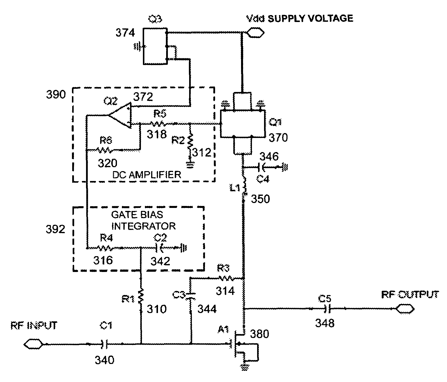
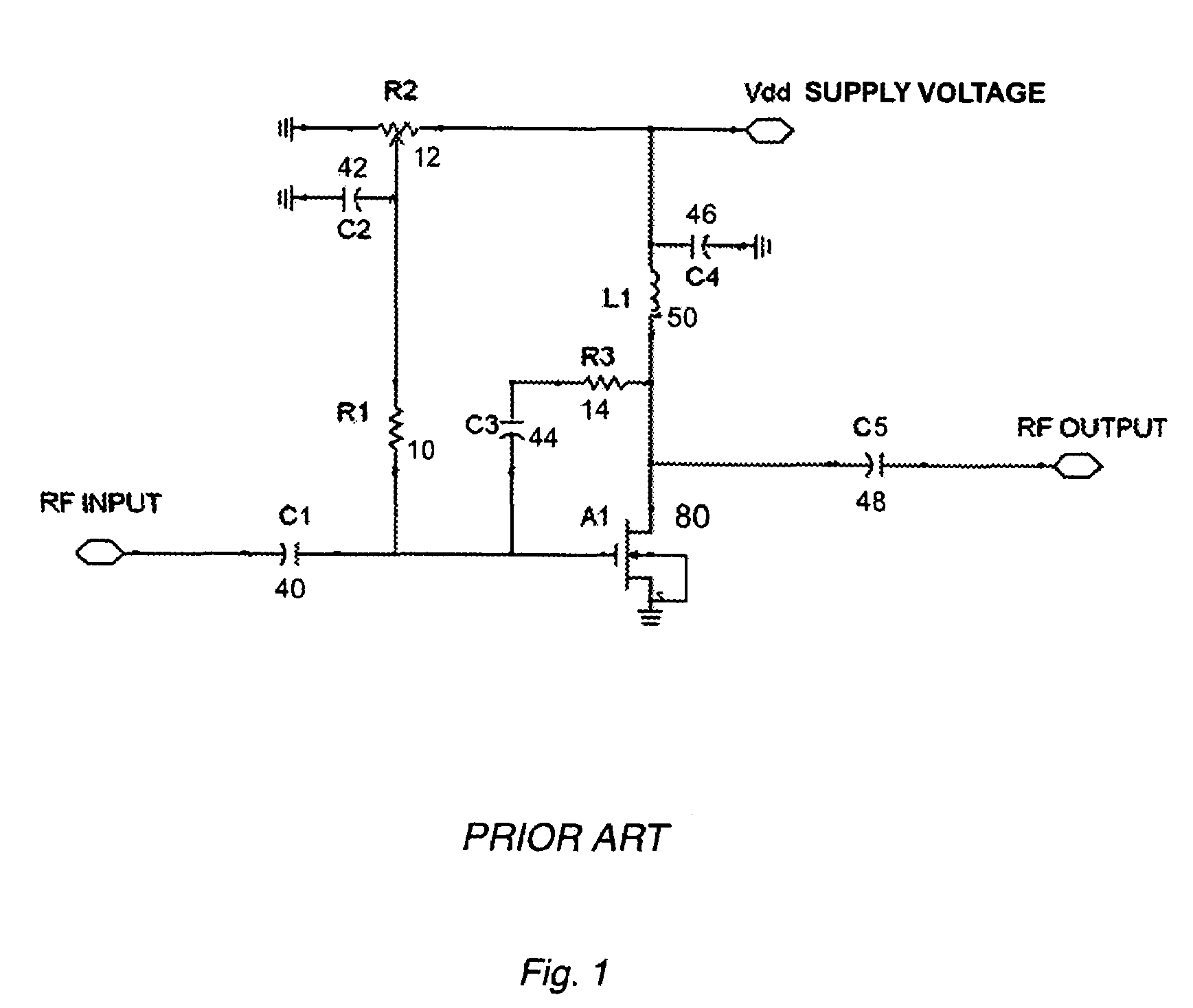
[0038]FIG. 1 shows a schematic of an output amplifier stage with a potentiometer-controlled gate bias circuit. The FET A180 requires the following components for normal operation. Capacitors C140 and C548 are DC blocking input and output capacitors. Resistor R110 and capacitor C242 are required for the application of a DC bias voltage to the gate of the transistor A180. Resistor R314 and capacitor C344 provide RF negative feedback. Inductor L150 functions as an RF choke. Capacitor C446 is a bypass capacitor on one end of the RF choke L150. Resistor R212 is the potentiometer that provides an adjustment for the gate voltage. The circuit of FIG. 1 has no stabilization of the gate voltage and relies completely on the voltage stability of the drain supply.

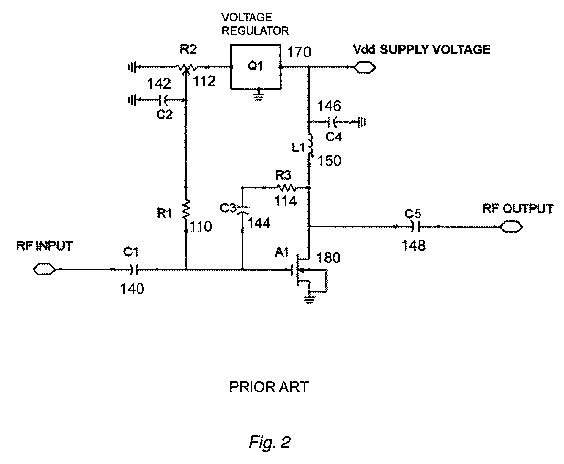
[0039]FIG. 2 shows a schematic of an output amplifier stage with a voltage regulator and potentiometer-controlled gate bias circuit. The voltage regulator Q1170 supplies a fixed voltage output that is divided by potentiometer R2112. Oth...


PUM


Abstract

A transistor biasing circuit is shown that utilizes a negative feedback loop control circuit to set the gate bias voltage in the output transistors of a power amplifier. This control circuit has a current sensor in series with the drain of the transistor, the current sensor output in turn feeding a dc signal into a dc amplifier, and the output of the dc amplifier driving a gate bias integrator which forms a dc control loop for maintaining the bias point. The output transistor is protected from excessive temperature and/or excessive power dissipation.

Description

BACKGROUND OF THE INVENTION[0001]1. Field of the Invention[0002]The present invention relates to an apparatus and a method for automatically controlling the gate bias voltage for Field Effect Transistor (FET) devices, and, more particularly in FET high power amplifiers.[0003]2. Description of the Prior Art[0004]High power amplifier circuits often use FETs in their output and driver stages. Generally, VDMOS (vertical double-diffused MOS) FET transistors are used for frequencies up to 500 MHZ and LDMOS (laterally diffused MOS) FET transistors are used for frequencies above 500 MHZ. For the best linearity, these high power amplifiers typically operate in Class A mode. Class A amplifiers are defined as having current flowing in all of the output transistors for the entire 360 degrees of an input cycle at the full, unclipped output of the amplifier. To achieve this, the output stage is biased halfway between the cutoff value and the saturation value and the load impedance is set at a val...

Claims


Application Information

Patent Timeline
IPC IPC(8): H02H7/20
CPCH03F1/301H03F1/523H03F3/193H03F2200/18
Inventor MORDKOVICH, MIKHAIL
Owner SCI COMPONENTS
Why Eureka
Try Eureka