Self-biased high-speed receiver

a receiver and high-speed technology, applied in the field ofmos integrated circuits, can solve problems such as circuit failure, core circuit damage or deformation, and circuit failure to work correctly, and achieve the effects of improving the response to high-speed io signals, stable bias voltage, and minimizing the number of devices working

Inactive Publication Date: 2008-03-25
TAIWAN SEMICON MFG CO LTD
View PDF13 Cites 11 Cited by
  • Summary
  • Abstract
  • Description
  • Claims
  • Application Information

AI Technical Summary

Benefits of technology

[0009]The preferred embodiment of the present invention is devised to provide an integrated solution of a high-speed IO signal receiver. A circuit with dual power supplies is described. The circuit has a self-biased circuit to provide a stable bias voltage. A reference voltage is provided to decide the state of an IO signal. Thick oxide transistors are used together with thin oxide transistors to match different operation voltages. The output signal has an amplitude of the core operation voltage. The integration of the signal receiver with the level-down converter minimizes the number of devices working under the high IO operation voltage and increases the work range of the receiver to a higher speed.
[0010]A variation of the high-speed signal receiver takes advantage of the very low threshold voltages of native transistors. The using of native thick oxide transistors extends the working range of the receiver to low command mode input signals.

Problems solved by technology

Problems can arise when a high IO signal with the amplitude Vddio is input to a core circuit.
The core circuit can be damaged or degraded if it is only designed to handle a voltage no higher than its operation voltage Vdd.
However, in deep micron technology, since the power voltage at node C is around 1V, while the input IO signal at node B is 2.5V to 3.3V, the circuit does not function correctly.
Transistors 1b and 2b and surrounding transistors may be damaged or degraded by voltages higher than they are designed to handle.
This not only increases power consumption but also degrades the circuit response to high-speed IO signals.
Firstly, charging a device to a higher voltage and discharging it requires more time, but the high-speed signals have only a short time to change state, so that the signals may be distorted.
Secondly, an IO signal is a noise source.
When a signal changes state, electromagnetic noise that interferes with other parts of the circuit are generated.
A higher voltage will generate a higher amount of noise.

Method used


Image

  • Self-biased high-speed receiver
  • Self-biased high-speed receiver
  • Self-biased high-speed receiver

Examples


Embodiment Construction

[0017]The making and using of the presently preferred embodiments are discussed in detail below. It should be appreciated, however, that the present invention provides many applicable inventive concepts that can be embodied in a wide variety of specific contexts. The specific embodiments discussed are merely illustrative of specific ways to make and use the invention, and do not limit the scope of the invention.

[0018]A preferred embodiment of a self-biased high-speed receiver is described. A variation of the present invention will then be discussed.

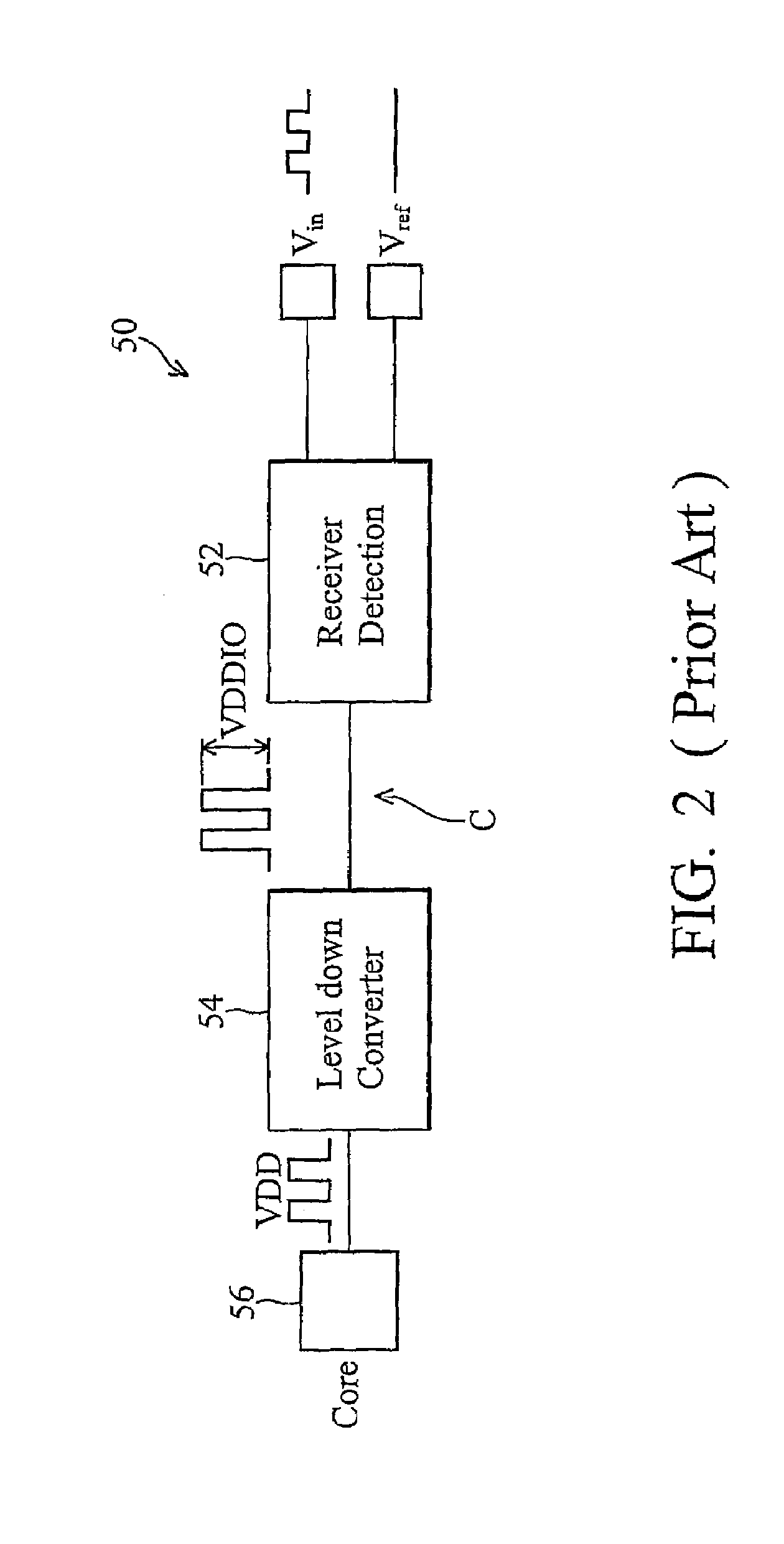
[0019]FIG. 3 illustrates a block diagram of a first embodiment of the present invention. Compared to FIG. 2, it is noted that the IO signal detector 53 and the level-down converter 54 are integrated into one circuit 60 and the intermediate IO signal with amplitude of Vddio is removed. The output of the circuit 60 is provided to a core circuit 56 compatible signal with the amplitude of Vdd.

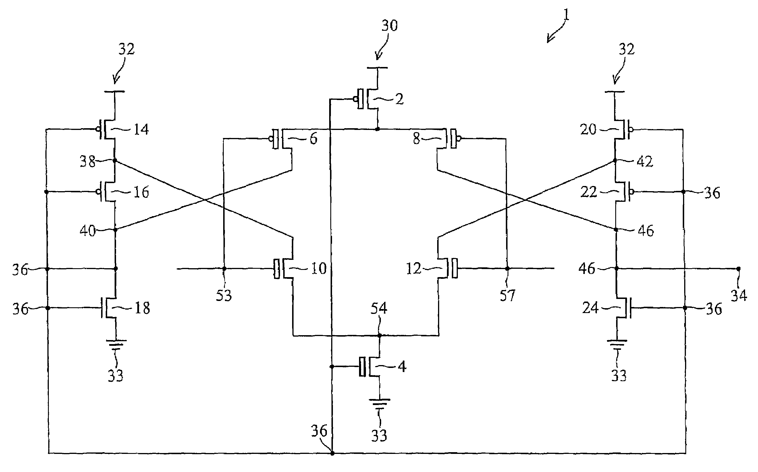
[0020]FIG. 4 illustrates a circuit schematic diagr...


PUM


Abstract

A self-biased high-speed receiver is described. The receiver is powered by one power supply with the core operation voltage and one power supply with the IO operation voltage. The receiver is self-biased to provide a stable bias voltage. A reference voltage and an IO signal are applied on the receiver so that the difference is amplified. Thick oxide transistors are used to increase the operation voltage of the transistors. Native thick oxide transistors are used so that the receiver can work with low command mode input.

Description

FIELD OF INVENTION[0001]This invention relates generally to the MOS integrated circuits and more particularly to a high-speed IO signal receiver that can be used in deep submicron technology.BACKGROUND[0002]An IO signal can be received by a receiver that detects the IO signal and amplifies it. The IO signal is then input to a core circuit for further processing. Since the IO signal is not generated by the core circuit, its amplitude is not limited by the core circuit's power supply voltage (also known as the core operation voltage or Vdd). The amplitude of the IO signal may be as high as the IO circuit's power supply voltage (also known as the IO operation voltage or Vddio). Therefore, the core circuit that directly takes input from an IO signal receiver must be able to handle an IO signal with amplitude of Vddio.[0003]In a traditional circuit that employs micron technology or earlier technologies, the operation voltage of the core circuit was in a range of about 2.5V to 3.3V, simil...

Claims


Application Information

Patent Timeline
Patent Type & Authority Patents(United States)
IPC IPC(8): H04B1/16G05F1/10G11C5/14H03F3/45
CPCH03K19/00315H03K19/00384H03K19/018528
Inventor OU, CHIUNG-TING
Owner TAIWAN SEMICON MFG CO LTD
Why Eureka
Try Eureka