Wired circuit board
a wired circuit board and wire technology, applied in the direction of printed circuit aspects, printed circuit manufacturing, electrical apparatus construction details, etc., can solve the problems of preventing the occurrence of insulating failure, etc., to suppress insulating failure, prevent short circuit from ionic migration, and improve adhesion
- Summary
- Abstract
- Description
- Claims
- Application Information
AI Technical Summary
Benefits of technology
Problems solved by technology
Method used
Image
Examples
example 1
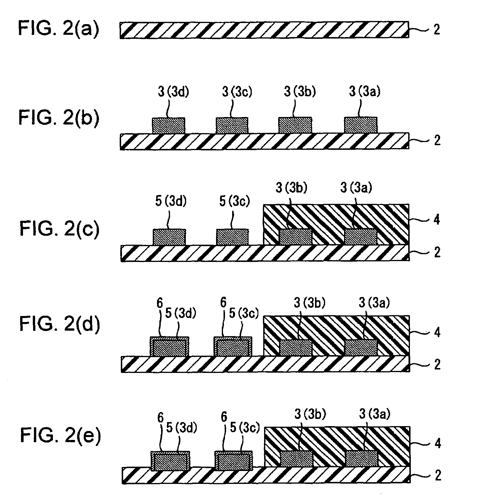
[0071]An insulating base layer formed by a polyimide resin film having a thickness of 25 μm and a glass transition temperature of 230° C. was prepared, first (Cf. FIG. 2(a)).
[0072]Then, a thin metal film was formed on the insulating base layer by sputtering a thin chromium film having a thickness of 0.03 μm and a thin copper film having a thickness of 0.10 μm sequentially. Then, a plating resist of a reverse pattern to the conductive pattern was formed on the thin metal film. Thereafter, a conductive pattern formed from copper was formed by electrolytic copper plating on a surface of the insulating base layer exposed from the plating resist. Thereafter, the plating resist was stripped and then the thin metal film exposed from the conductive pattern was removed by wet etching. As a result, the conductive pattern having a thickness of 10 μm was formed in a pattern comprising a plurality of wires which were spaced from each other at a distance of 30 μm (Cf. FIG. 2(b)).
[0073]Then, varni...
example 2
[0076]An insulating base layer formed by laminating an insulating over layer formed by a polyimide resin film having a thickness of 5 μm and a glass transition temperature of 230° C. on an insulating under layer formed by a polyimide resin film having a thickness of 20 μm and a glass transition temperature of 350° C. was prepared (Cf. FIG. 3(b)).
[0077]Then, a conductive pattern having a thickness of 10 μm was formed in a pattern comprising a plurality of wires spaced from each other at a distance of 30 μm in the same manner as in Example 1 (Cf. FIG. 3(c)).
[0078]Further, an insulating cover layer, formed by a polyimide resin having a thickness of 15 μm, for covering the conductive pattern was formed on the insulating base layer in the same manner as in Example 1 (Cf. FIG. 3(d)).
[0079]Then, a gold plating layer having a thickness of 0.5 μm was formed on surfaces of each terminal portion in the same manner as in Example 1 (Cf. FIG. 3(e)). Thereafter, the terminal portions were subjecte...
PUM
| Property | Measurement | Unit |
|---|---|---|
| Tg | aaaaa | aaaaa |
| thickness | aaaaa | aaaaa |
| thickness | aaaaa | aaaaa |
Abstract
Description
Claims
Application Information


