Complementary metal-oxide-semiconductor image sensor and method for fabricating the same
a metal-oxide-semiconductor and image sensor technology, applied in the field of complementary metal-oxide-semiconductor (cmos) image sensor, can solve the problems of critical error in the detection of electric signals, display screen whitening in a dark state, and use of polycide gate structure does not provide the intended level of operation speed
- Summary
- Abstract
- Description
- Claims
- Application Information
AI Technical Summary
Benefits of technology
Problems solved by technology
Method used
Image

Examples
first embodiment
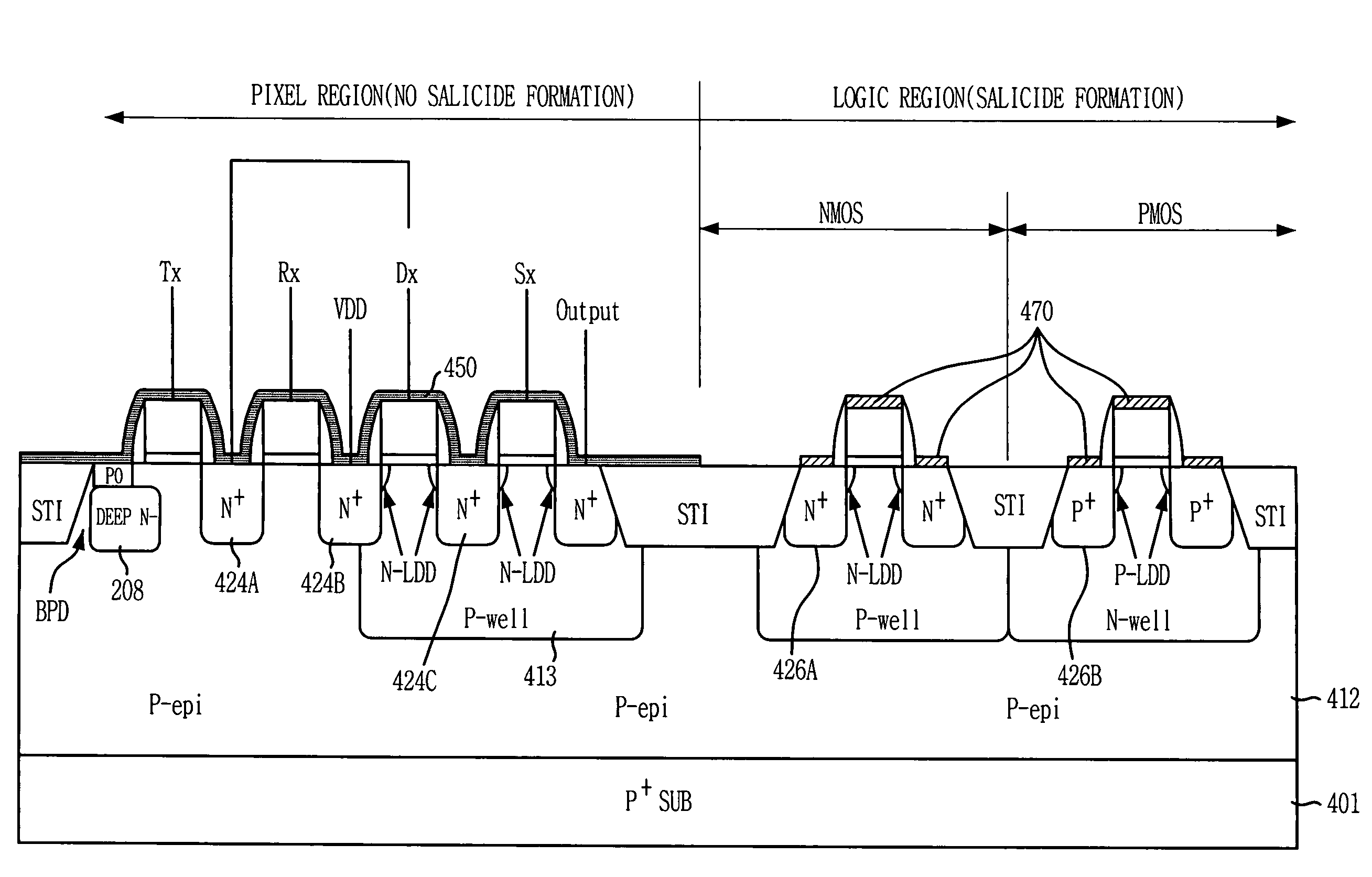
[0032]FIG. 4 is a cross-sectional view showing a CMOS image sensor in accordance with the present invention.
[0033]As shown, a salicide blocking layer 450 is formed on an entire pixel region including a buried photodiode BPD, an N+-type floating diffusion region 424A, which is a sensing node, and other devices configuring a unit pixel. In a logic region, a salicide layer 470 is formed on each gate of CMOS devices and highly doped N+-type impurity regions 426A and P+-type impurity diffusion regions 426B both serving as source / drain regions. Herein, the salicide layer is a self-aligned silicide layer.
[0034]If the silicide layer is formed on the source / drain regions in the logic region except for the pixel region, an operation speed of the CMOS image sensor that detects an electric signal corresponding to a photo-generated electric charge through a correlated double sampling mode can be enhanced. Also, being different from the conventional CMOS image sensor, the silicide layer does not ...
second embodiment
[0043]FIG. 5 is a cross-sectional view showing a CMOS image sensor in accordance with the present invention.
[0044]In the CMOS image sensor according to the second embodiment of the present invention, a salicide blocking layer 550 is formed on a buried photodiode (BPD), a gate of a transfer transistor Tx, an N+-type floating diffusion region 524A and a portion of a gate of a reset transistor Rx, while a salicide layer 570 is formed over those devices configuring a unit pixel in a pixel region and over CMOS devices in a logic region. That is, the salicide layer 570 is formed on gates of a driver transistor Dx, a select transistor Sx, an NMOS transistor, a PMOS transistor, an N+-type drain junction 524B, N+-type impurity diffusion regions 524C and N+-type and P+-type impurity diffusion regions 526A and 526B. It should be noted that a CMOS image sensor fabrication method according to the second embodiment is identical to the CMOS image sensor fabrication method described in the first em...
PUM
 Abstract
Description
Claims
Application Information
 - R&D
- Intellectual Property
- Life Sciences
- Materials
- Tech Scout
- Unparalleled Data Quality
- Higher Quality Content
- 60% Fewer Hallucinations
Browse by: Latest US Patents, China's latest patents, Technical Efficacy Thesaurus, Application Domain, Technology Topic, Popular Technical Reports.
© 2025 PatSnap. All rights reserved.Legal|Privacy policy|Modern Slavery Act Transparency Statement|Sitemap|About US| Contact US: help@patsnap.com