Radiation tolerant electrostatic discharge protection networks

a technology of protection network and electrostatic discharge, which is applied in the direction of radiation hardening, pulse technique, transistors, etc., can solve the problems that the electrostatic discharge network poses a hazard to the integrity of the circuitry in spa

Inactive Publication Date: 2008-04-15
IBM CORP
View PDF12 Cites 7 Cited by
  • Summary
  • Abstract
  • Description
  • Claims
  • Application Information

AI Technical Summary

Problems solved by technology

These needs and others are satisfied by first realizing that electrostatic discharge networks pose a hazard to the integrity of the circuitry in space.

Method used


Image

  • Radiation tolerant electrostatic discharge protection networks
  • Radiation tolerant electrostatic discharge protection networks
  • Radiation tolerant electrostatic discharge protection networks

Examples


Embodiment Construction

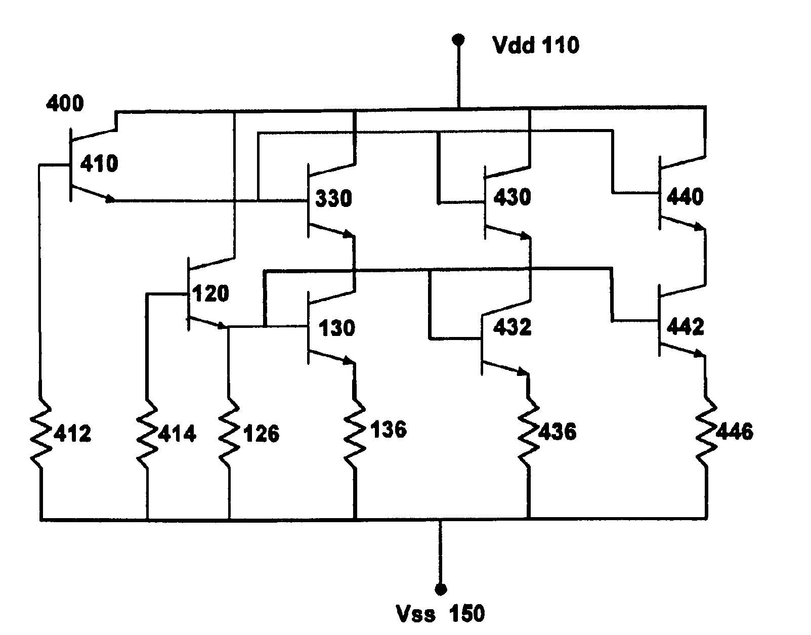
[0022]As discussed earlier, the collision of heavy ion particles often leads to secondary breakdown events in space caused by high energy protons and neutrons colliding with the silicon lattice of electronic circuits leading to fission fragments and damage to the electronic devices. Electrostatic discharge networks (ESD) can be used to quickly remove power from a circuit resulting from bombardment by cosmic rays but when the ESD network itself is hit, then catastrophic failure may occur because of excessive heat, or metallization or bond failure. Bipolar-based ESD networks, moreover, actually fail in space applications. Hereinafter the distinction between SEUs, SELs, and SEBs shall be merged and the event, whether it be a latch-up or a burn-out, shall simply be referred to a single event upset (SEU). Until now, the failure of ESD networks in space from SEUs has not been addressed.

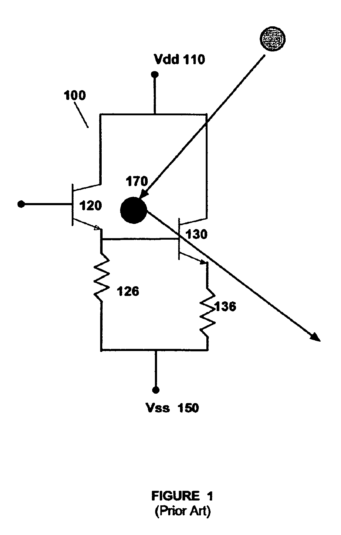
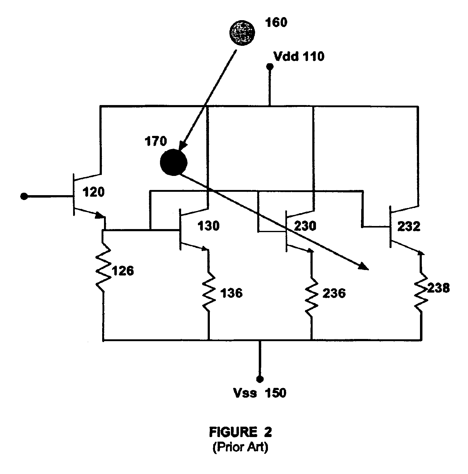
[0023]FIG. 1 is a schematic of a prior art silicon germanium power clamp 100 that limits the current in ...


PUM


Abstract

Realizing that rather than protect electronic circuitry, electrostatic discharge networks when hit by cosmic rays and charged particles, can actually cause the electronic circuitry in satellites and other space applications to fail, the inventor created an ESD network having a redundant voltage clamping element in series with a first voltage clamping element between two voltage pads. The ESD network may be connected to a power voltage pad or a signal voltage pad either directly or through a dummy voltage pad. The voltage clamping elements may further comprise an array of unit cells wherein the array is electrically equivalent to single large transistors currently used in ESD networks. By creating an ESD network as an array of unit cells, benefits greater than those obtained by using a single transistor as a clamping or a trigger element are realized—such as increased ballast resistance and less overall damage to the circuitry resulting from cosmic rays and particles.

Description

FIELD OF THE INVENTION[0001]This invention relates generally to the field of protection of semiconductor circuits from radiation effects, and in particular relates to creating electrostatic discharge (ESD) circuits that are tolerant of single event upsets.BACKGROUND OF THE INVENTION[0002]Semiconductor circuits are composed of a regular arrangement of atoms, usually silicon. In semiconductors, the arrangement of the atoms are often in a lattice or mesh arrangement and the electrons and the holes created by the lack of electrons are free to move within planes of the lattice. As semiconductor devices become smaller and smaller, fewer and fewer atoms are used to create an electronic device. Transistors of semiconductor materials often store sufficient charge to create digital information by storing a 0 or a 1 state depending upon the threshold voltage of the transistor.[0003]The primary component of nature is space and so there is mostly space between the atoms in a semiconductor lattic...

Claims


Application Information

Patent Timeline
Patent Type & Authority Patents(United States)
IPC IPC(8): H01L23/62
CPCH01L27/0259H03K19/0033H03K19/00338H01L2924/0002H01L2924/00
Inventor VOLDMAN, STEVEN H.
Owner IBM CORP
Why Eureka
Try Eureka