Method for forming elements with reduced variation

a technology of variation and forming elements, applied in the direction of amplifier details, differential amplifiers, amplifiers with semiconductor devices/discharge tubes, etc., can solve the problems of error voltage, performance limitation aspect of all practical amplifiers, and unbalance of practical differential amplifiers, so as to reduce possible operating parameter mismatches

Active Publication Date: 2008-04-15
ELDER J SCOTT
View PDF18 Cites 20 Cited by
  • Summary
  • Abstract
  • Description
  • Claims
  • Application Information

AI Technical Summary

Benefits of technology

[0037]According to one embodiment, the present invention comprises a method for reducing possible operating parameter mismatch between first and second elements. The method comprises fabricating a plurality of like components each functionally similar to the first and the second elements, selecting components from the plurality of like components and interconnecting the selected components to construct the first element as a composite element, wherein the operating parameter mismatch between the composite element and the second element is limited based on assessment of operating parameter variation among the like components.

Problems solved by technology

However, a practical differential amplifier exhibits an unbalance caused by mismatches in the characteristics of the two input transistors.
This error voltage is a performance limiting aspect of all practical amplifiers.
In practice this is not always possible.
The mismatch of integrated elements manufactured according to a well-designed semiconductor process is a result of random manufacturing imperfections.
These manufacturing imperfections include many factors such as lithography errors, process gradients, and chemical etching rate variations, among others.
These additional circuit elements not only add materials cost to the production of a system, but they also add labor costs since time is required to perform the calibration.
Furthermore, if the circuit elements used for calibrating are not precisely the same as those used in the primary matching circuit, the performance of the calibration will degrade as operating environments change since dissimilar elements exhibit dissimilar drift characteristics.
Fifteen-millivolts of input offset voltage is considered poor by those skilled in the art of precision analog amplifier design.
Such a poor specification is not indicative of a high precision amplifier design.
Furthermore, it is well understood by those skilled in the art that any calibration of such a large error will not be well maintained over environmental changes, such as time and temperature, during amplifier operation.
However, using a large physical structure on a silicon die is an expensive solution to achieve matching since this adds materials cost.
In many cases it further degrades other equally important performance specifications.
When the gate electrode of a MOS transistor is formed during manufacturing, a multiplicity of random error-generating events occur such that the gate electrode is not formed with a perfectly flat edge along the width of the MOS channel.
These random events include, among other things, photolithographic errors and gate electrode etching rate variations.
The depiction of the transistor mismatch error source shown in FIGS. 4A and 4B is greatly exaggerated and an over simplification of the manufacturing anomalies that lead to mismatched performance between identically sized MOS transistors manufactured simultaneously.
There are numerous other manufacturing abnormalities that contribute to the mismatch of MOS transistors.
It is the accumulation of all manufacturing error sources during MOS transistor manufacturing that result in MOS transistor pair mismatch.
While time averaging solutions such as DEM and chopper stabilization are able to theoretically mask all vestiges of element mismatch in an analog circuit, many precision amplifier applications cannot tolerate the byproducts of a clock signal injected into the signal path.
Two intolerable byproducts are long overload recovery time when the amplifier is driven into saturation and the introduction of switching noise into the signal path.
Additionally, errors that drift faster than the amplifiers response time are not eliminated and therefore add error to the output in a manner similar to that produced by element mismatch.
Cherry-picking is an extremely inefficient and costly solution in that a multiplicity of completed elements must be included on the die with the end result that only one will be utilized.

Method used


Image

  • Method for forming elements with reduced variation
  • Method for forming elements with reduced variation
  • Method for forming elements with reduced variation

Examples


Embodiment Construction

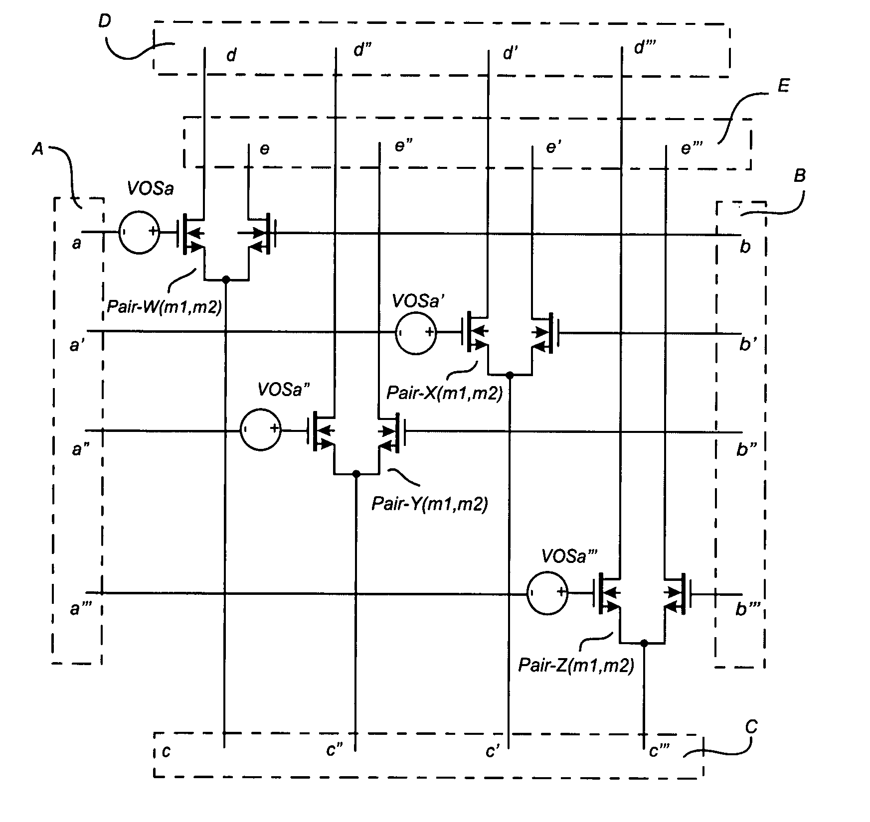
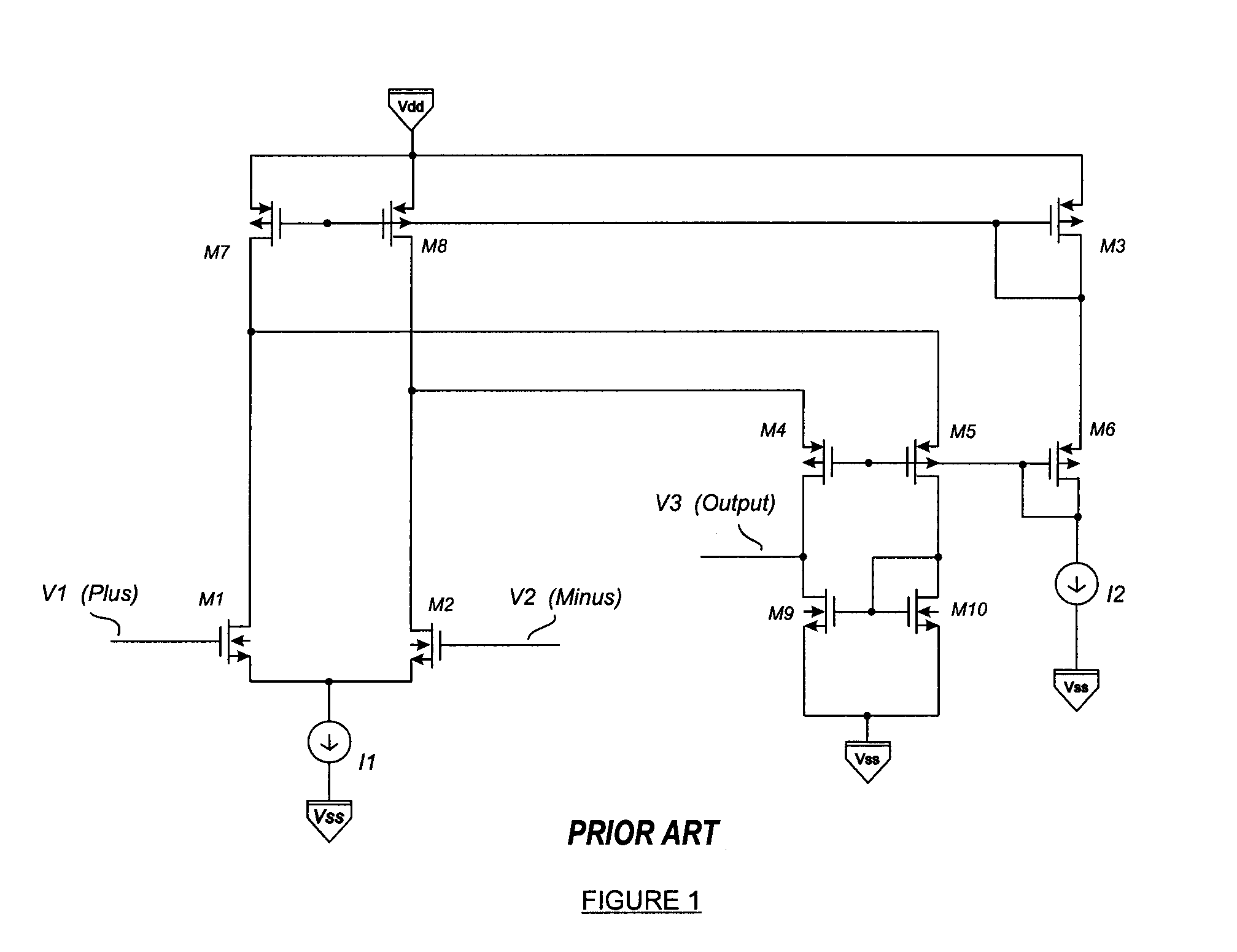
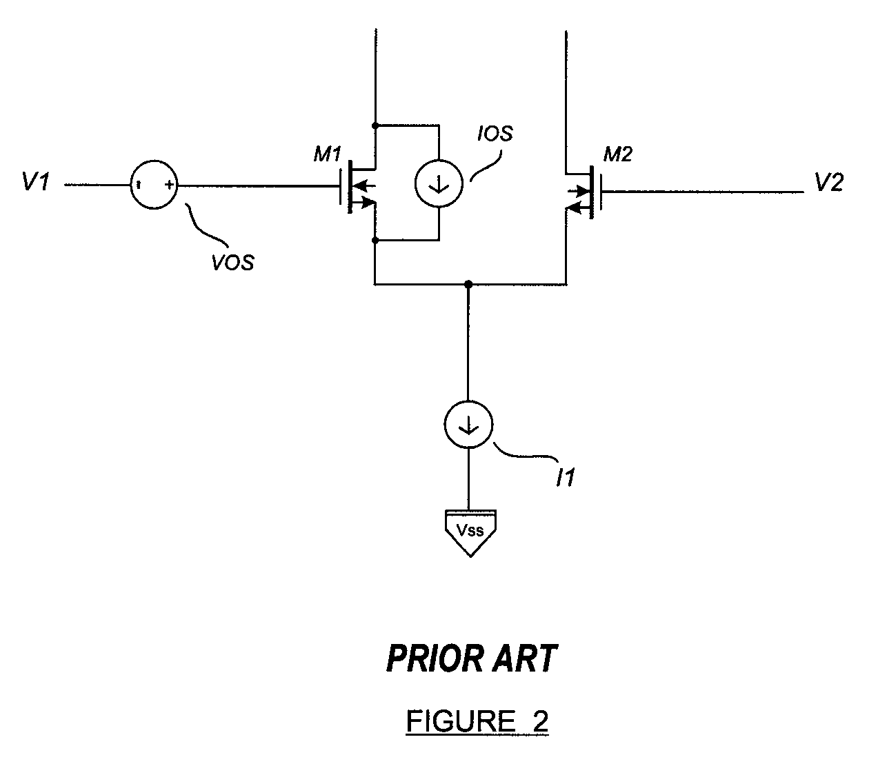
[0069]Before describing in detail the particular methods and apparatuses related to calibrating analog circuits using statistical techniques and overcoming the effects of component mismatches it should be observed that the present invention resides primarily in a novel and non-obvious combination of elements and process steps. So as not to obscure the disclosure with details that will be readily apparent to those skilled in the art, certain conventional elements and steps have been presented with lesser detail, while the drawings and the specification describe in greater detail other elements and steps pertinent to understanding the invention.

[0070]The following embodiments are not intended to define limits as to the structure or method of the invention, but only to provide exemplary constructions. The embodiments are permissive rather than mandatory and illustrative rather than exhaustive.

[0071]High performance analog integrated circuits frequently require post-manufacturing calibr...


PUM


Abstract

The performance of precision analog integrated electronic circuits is directly related to the degree of matching between electrical circuit elements. Any residual mismatch of circuit elements after manufacturing must be calibrated out using numerous techniques such as adjusting potentiometers, trimming capacitors, modifying binary-weighted resistor strings, etc. Prior art matching techniques entail the use of large area circuit elements or a large number of elements arranged in a prescribed manner on the surface of a silicon die to minimize the residual calibration. The present invention utilizes a multiplicity of circuit elements that are interconnected in distinct groups to achieve a higher degree of element matching and the ensuing benefits thereof. The elements are interconnected to yield a prescribed minimum mismatch error.

Description

[0001]This application claims the benefit of U.S. Provisional Patent Application No. 60 / 625,862 filed on Nov. 8, 2004.TECHNICAL FIELD OF THE INVENTION[0002]This invention relates generally to methods and apparatuses for calibrating precision analog integrated electronic systems. In particular, this invention details novel and non-obvious methods and apparatuses for calibrating out manufacturing errors inherent in high precision, analog integrated circuits. While the invention described herein is discussed in terms of analog integrated electronic circuits, the invention is further applicable to the calibration of any physical product where precise control of a relationship between elements is required. In the case of analog integrated circuits, the calibration of product specifications such as operational amplifier input offset voltage, offset voltage drift, bandgap voltage reference tolerance, operational amplifier common-mode and power supply rejection ratios and others can benefit...

Claims


Application Information

Patent Timeline
Patent Type & Authority Patents(United States)
IPC IPC(8): H03F3/45
CPCH03F1/30H03F1/301H03F1/526H03F3/45H03F3/45192H03F3/45744H03F3/45766H03F3/70H03F2200/261H03F2203/45028H03F2203/45048H03F2203/45538
Inventor ELDER, J. SCOTT
Owner ELDER J SCOTT
Why Eureka
Try Eureka