Electroabsorption modulator and method of manufacturing the same

a technology of electroabsorption modulator and manufacturing method, which is applied in the direction of instruments, non-linear optics, optical elements, etc., can solve the problems of limiting the speed of the electroabsorption modulator that maintains a certain extinction ratio, the slope of the transfer function should be steep, and the need for optical modulators, etc., to achieve low optical coupling loss and high input optical power

Inactive Publication Date: 2008-04-15
ELECTRONICS & TELECOMM RES INST
View PDF8 Cites 20 Cited by
  • Summary
  • Abstract
  • Description
  • Claims
  • Application Information

AI Technical Summary

Benefits of technology

[0020]The present invention is directed to an electroabsorption modulator which has a low optical coupling loss with an optical fiber and is operable in a relatively high input optical power.
[0021]One aspect of the present invention is to provide a double waveguide type electroabsorption modulator including: a first optical waveguide in which light is modulated and a second optical waveguide that facilitates optical coupling with an optical fiber; and first and second spot size converters located between the first and second optical waveguides for changing and moving the optical mode, wherein an optical confinement factor is adjusted according to a thickness of the second spot size converter.

Problems solved by technology

Therefore, not only the analog optical modulator is required to operate in high input optical power but also the slope of its transfer function should be steep.
Consequently, there is a limit in the speed of the electroabsorption modulator that maintains a certain extinction ratio.
In this case, when light having large intensity is incident, a phenomenon occurs that a very large current is generated at the front portion of the device to break down the device.
Likewise, a typical optical modulator having a high OCF to increase optical modulation efficiency cannot operate properly when light having large intensity is input, and, from the viewpoint of the traveling wave optical modulator, the electrical signals are distributed along the optical waveguide while the optical signals are absorbed in the front portion, thus resulting in a negligible difference from a lumped device.
Most insertion loss is caused by the optical coupling loss with the optical fiber, which is generated from inconsistency of an optical mode between the semiconductor optical device and the optical fiber.
Therefore, in optical coupling between the semiconductor optical device and the optical fiber, a very large loss is unavoidable due to the mismatch of the optical mode size.
This arrangement has problems in that the epitaxial re-growth is required in the SAG method, and that the SAG method itself applies a stress to a semiconductor crystal.
Thus, there is a problem in that the growth conditions are complicated and should be strictly regulated.
However, this method has also drawbacks in that the manufacture process is complicated by the use of the SAG method.
Therefore, even with very high input optical power, an amount of optical current generated by input light absorption in the absorption layer is substantially very low.
However, this technology is inappropriate to the digital optical communication, because most of the optical modes exist below the absorption layer and thus a sufficient extinction ratio cannot be obtained.
Further, although the size of the optical mode is increased, the shape is still elliptical, resulting in an optical coupling loss with the circular optical fiber.
However, there are drawbacks in that the SAG method has a complicated manufacturing process, strict processing conditions, and is difficult to manufacture, and that the PCW structure cannot have a sufficient extinction ratio.

Method used


Image

  • Electroabsorption modulator and method of manufacturing the same
  • Electroabsorption modulator and method of manufacturing the same
  • Electroabsorption modulator and method of manufacturing the same

Examples


Embodiment Construction

[0035]The present invention will now be described more fully hereinafter with reference to FIGS. 1 to 6, in which preferred embodiments of the invention are shown. This invention may, however, be embodied in different forms and should not be construed as limited to the embodiments set forth herein. Rather, these embodiments are provided so that this disclosure will be thorough and complete, and will fully convey the scope of the invention to those skilled in the art.

[0036](Electroabsorption Modulator)

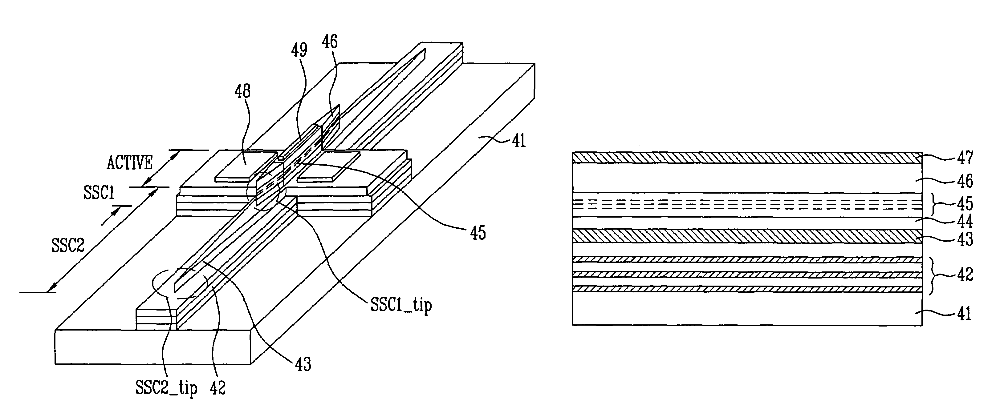
[0037]FIG. 1A is a perspective view of an spot size converter integrated electroabsorption modulator according to an embodiment of the present invention, and FIG. 1B is a schematic cross-sectional view of FIG. 1A.

[0038]Referring to FIG. 1A, a double waveguide electroabsorption modulator includes first and second optical waveguides 45 and 42, and first and second spot size converters SSC1 and SSC2 located therebetween for changing and moving an optical mode. An optical confinement factor...


PUM


Abstract

Provided is a double waveguide electroabsorption modulator, in which two spot size converters are integrated between first and second optical waveguides, thereby reducing an insertion loss between an optical fiber and an optical modulator while favorably operating even in high input optical power. Therefore, the electroabsorption modulator can stably operate in higher input optical power while reducing an optical coupling loss and an optical confinement factor (OCF).

Description

CROSS-REFERENCE TO RELATED APPLICATION[0001]This application claims priority to and the benefit of Korean Patent Application No. 2004-105699, filed Dec. 14, 2004, the disclosure of which is incorporated herein by reference in its entirety.BACKGROUND[0002]1. Field of the Invention[0003]The present invention relates to an electroabsorption modulator, and more specifically, to an electroabsorption modulator appropriate for analog optical communication in which an optical waveguide and an spot size converter are integrated with each other to reduce an insertion loss between an optical fiber and an optical modulator and to favorably operate in high input optical power, and a method of manufacturing the same.[0004]2. Discussion of Related Art[0005]In general, an electroabsorption modulator used for modulating signals in digital optical communication serves to adjust an intensity of output light according to an electrical signal input by interrupting an intensity of incident light (referre...

Claims


Application Information

Patent Timeline
Patent Type & Authority Patents(United States)
IPC IPC(8): G02B6/12H01L21/00
CPCB82Y20/00G02B6/1228G02B6/136G02F1/01708G02B2006/12176G02B2006/12128
Inventor KANG, YOUNG SHIKKIM, JEHAKWON, YONG HWANCHUNG, YONG DUCK
Owner ELECTRONICS & TELECOMM RES INST
Why Eureka
Try Eureka