Atomic read/write support in a multi-module memory configuration

a multi-module memory and support technology, applied in the field of processor complexes, can solve the problems of reducing the bandwidth to and from the memory system, exacerbate the problem, and affecting the performance of the memory system, so as to increase the bandwidth between the processors and the processors without adverse effects

Active Publication Date: 2008-04-15
META PLATFORMS INC
View PDF10 Cites 23 Cited by
  • Summary
  • Abstract
  • Description
  • Claims
  • Application Information

AI Technical Summary

Benefits of technology

[0020]One advantage of the invention is that processors can independently access a block of data in a common memory device without adversely affecting any other processor which also has access to that memory device. In other words, multiple data blocks of different sizes can be accessed by different processors at the same time, while the accesses are atomic to each processor.
[0021]Another advantage is that latencies for processors waiting to access blocks of memory are reduced.
[0022]Still another advantage is that locking of large blocks of memory which may occur in the prior art devices is eliminated. In the present invention, a processor does not need to wait for other processors to unlock sections of memory, thereby increasing bandwidth between the processors and the memory system.
[0023]Yet another advantage is that information in a common memory device can be updated without interruption.
[0024]This invention allows accesses to different addresses for each bank during a window. Thus, simultaneous access to the same or different data block by different processors is possible.
[0025]These and other objects and advantages, which will become manifest upon reading and a full understanding of this invention, are achieved in the manner to be hereinafter described.

Problems solved by technology

In many cases, a block of data being accessed by one of the general purpose processors cannot fit into a single memory location or bank within a memory module, thereby necessitating the allocation of the data into different memory locations within the same module or in another module.
The problem is exacerbated by the fact that the data block may be spread across multiple banks of a DRAM module, and across multiple addresses (rows) in the module.
The same challenges are present in any system in which multiple processors attempt to independently access data blocks which are stored in a memory system comprised of multiple modules, DRAM and / or SRAM.
This method has a definite latency penalty.
This method degrades bandwidth to and from the memory system, since a data block may not include all banks of a DRAM module.

Method used


Image

  • Atomic read/write support in a multi-module memory configuration
  • Atomic read/write support in a multi-module memory configuration
  • Atomic read/write support in a multi-module memory configuration

Examples


Embodiment Construction

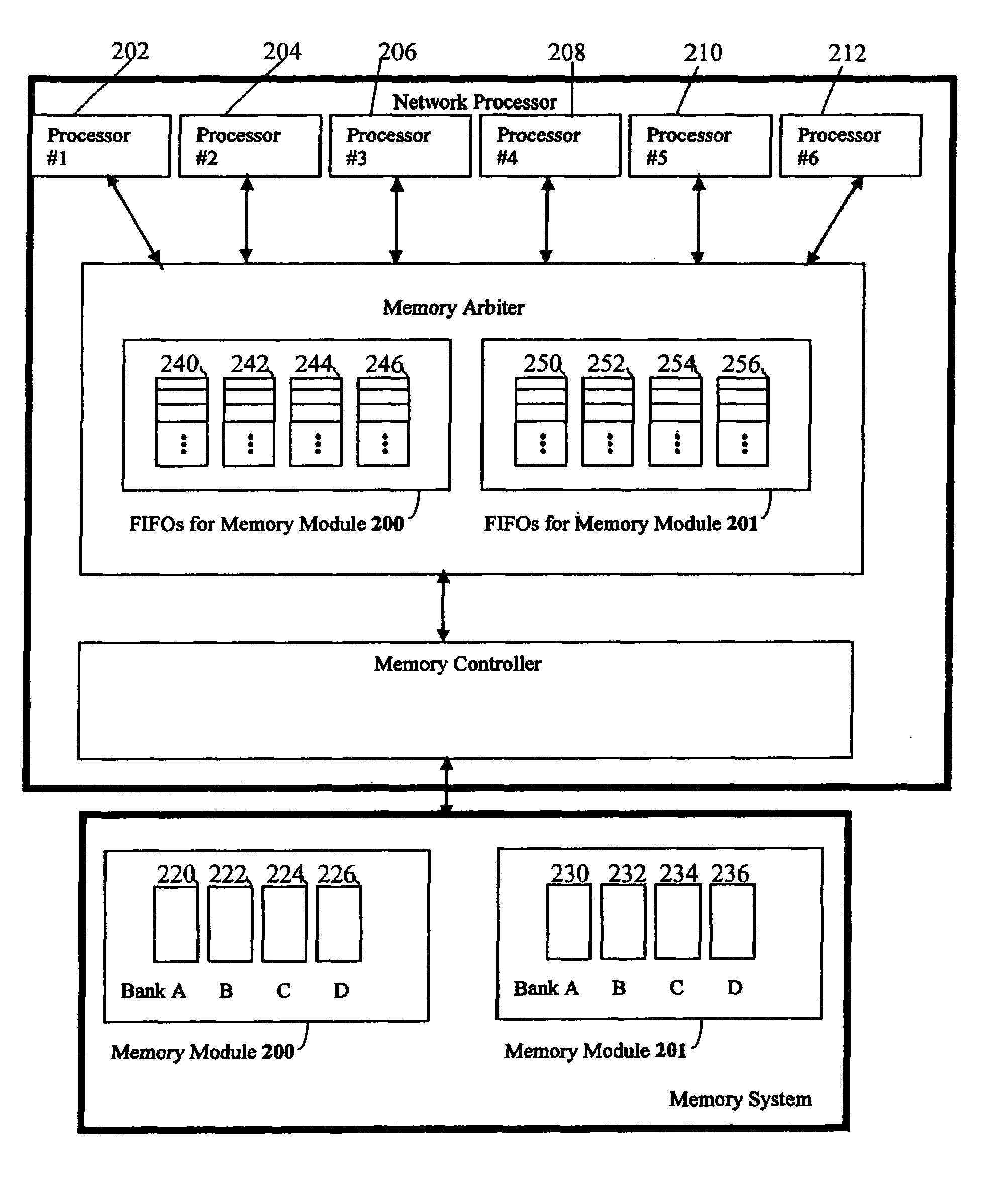
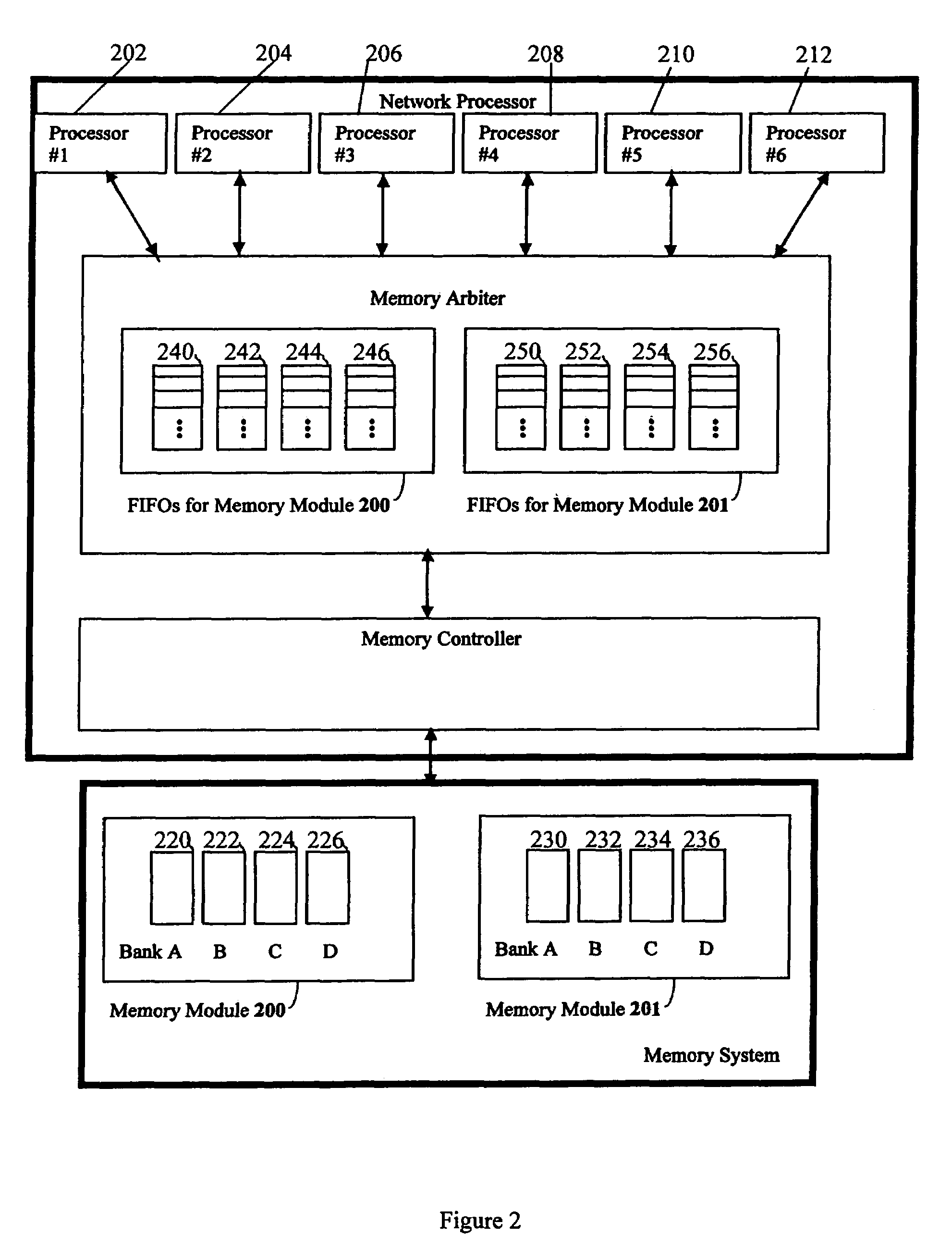
[0032]According to the present invention, an atomic read / write function is implemented per data block transferred, such that all the data in a data block requested by one processor from a given location in memory is transferred before the same data block is transferred to or from another processor. This procedure solves the stated problem with an atomic read and write function in the memory arbiter of the network processing chip.

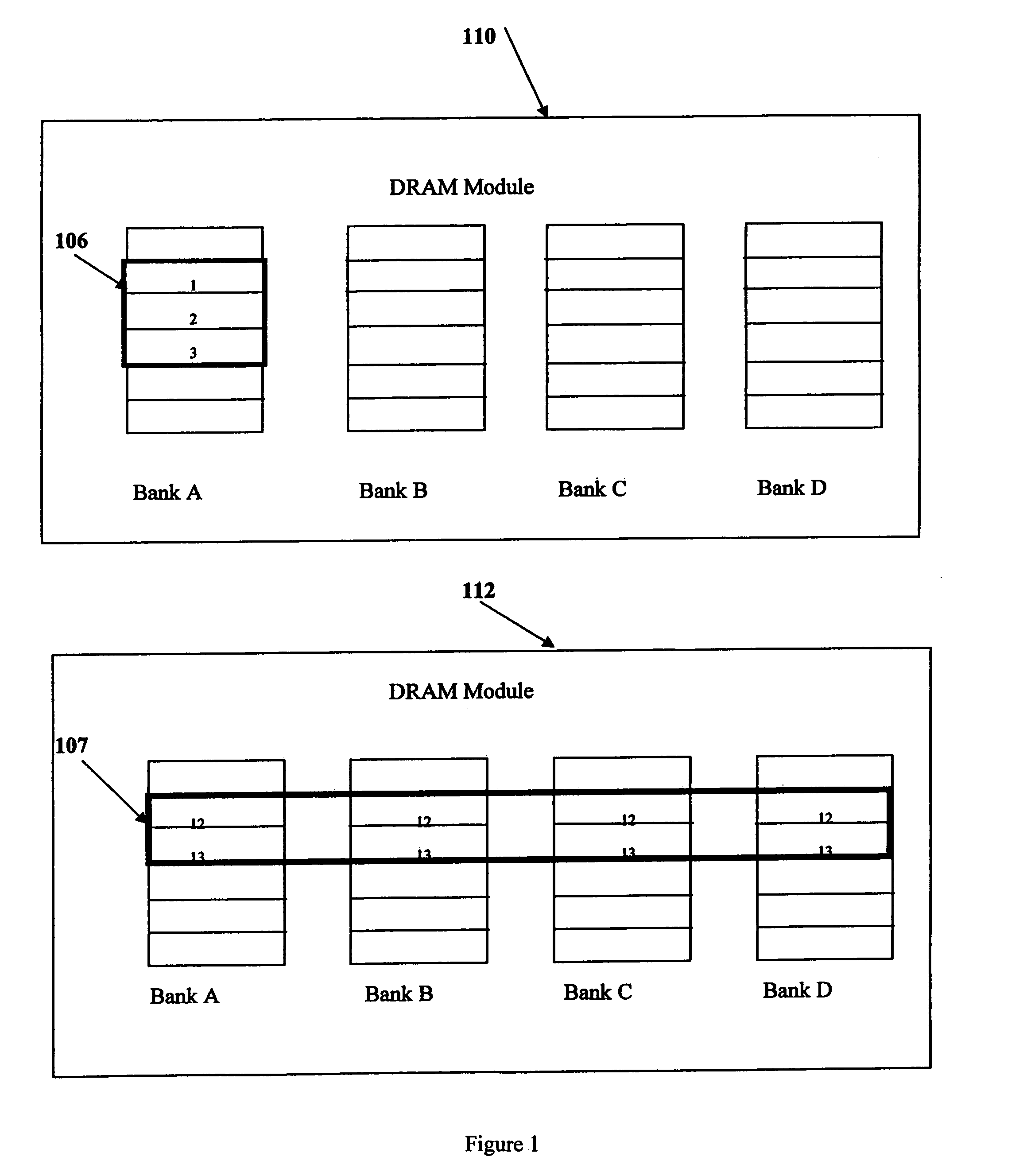
[0033]The invention is implemented in hardware, i.e. digital circuits, and no software is used. Each bank of each memory module has an associated FIFO buffer. Thus, each DRAM will have multiple FIFO buffers (four or eight depending on the DRAM module architecture). In memory systems containing SRAMs, each SRAM is viewed as having one bank and, thus, one FIFO buffer. It should be noted that a data block can span multiple SRAMs, and can span SRAMs plus DRAMs, depending on the architecture of the memory system.

[0034]The general purpose processors, numbered 0 to...


PUM


Abstract

Efficient transfer of data to and from random access memory is described. Multiple request sources and a memory system comprise memory modules having memory banks, each bank containing rows of data. The retrieval comprises transferring all data pursuant to a given request by one source before any data is transferred pursuant to a subsequent request from said second source. This retrieval is achieved using a memory arbiter that implements an algorithm for atomic read / write. Each bank is assigned a FIFO buffer by the arbiter to store access requests. The access requests are arbitrated, and an encoded value of a winner of arbitration is loaded into the relevant FIFO buffer(s) before choosing the next winner. When an encoded value reaches the head of the buffer, all associated data is accessed in the given bank before accessing data for another request source.

Description

CROSS REFERENCE TO RELATED APPLICATIONS[0001]This invention is related to the following patents: namely, U.S. Pat. No. 6,460,120 B1, issued Oct. 1, 2002 entitled NETWORK PROCESSOR, MEMORY ORGANIZATION AND METHODS, and U.S. Pat. No. 6,463,500 B1, issued Oct. 8, 2002 entitled APPARATUS AND METHOD TO ACCESS COMPUTER MEMORY BY PROCESSING OBJECT DATA AS SUB-OBJECT AND SHAPE PARAMETER. The contents of each of these two patents are hereby incorporated by reference into the present description as fully as if they were represented herein in their entirety.FIELD OF THE INVENTION[0002]This invention relates generally to processor complexes and to their memory systems that store different size blocks of information data in memory modules. More particularly, it relates to the efficient accessing of data stored in dynamic random access memory modules and to a method for data access implemented in digital circuits.BACKGROUND OF THE INVENTION[0003]The discussion relating to the present invention wi...

Claims


Application Information

Patent Timeline
Patent Type & Authority Patents(United States)
IPC IPC(8): G06F13/00
CPCG06F13/1652
Inventor JENKINS, STEVEN K.WEAVER, LAURA A.
Owner META PLATFORMS INC
Why Eureka
Try Eureka