Circuit board and a power module employing the same
a technology of circuit board and power module, which is applied in the field of circuit board, can solve the problems of reducing the life of circuit boards, preventing the formation of desired circuit patterns, and unable to eliminate patterns with potential instability, so as to achieve precise and versatile effects, reduce the non-uniformity of chemical treatment, and reduce the effect of non-uniformity
- Summary
- Abstract
- Description
- Claims
- Application Information
AI Technical Summary
Benefits of technology
Problems solved by technology
Method used
Image


Examples
example 1
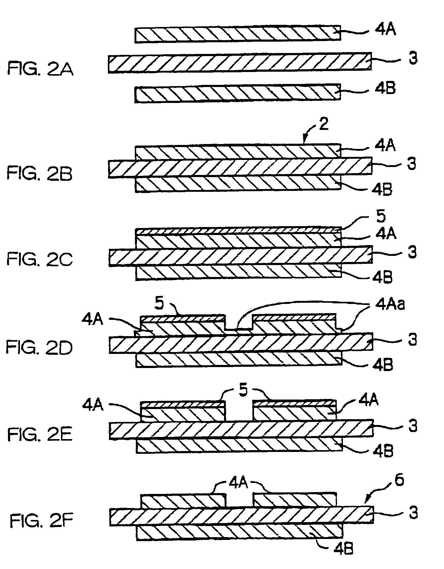
[0064]According to the scheme shown in FIGS. 2A-2F, a circuit pattern was formed on a metal-insulator composite member 2 employing a milling machine (product of MITS Co., Ltd.) In steps A and B, a ceramic substrate 3 made of aluminum nitride with a purity of at least 98.8% and which had a thickness of 0.635 mm was brought into contact with aluminum sheets 4A and 4B of identical shape and area at a thickness of 0.4 mm, 4A serving as a circuit forming metal layer and 4B as a heat sink providing metal layer; the assembly was heated in an inert atmosphere at 740° C. for 60 minutes and then cooled down (i.e. direct joining) to prepare a composite member 2. In step C, an etching resist 5 made of an acrylic resin was applied to the entire surface of the aluminum sheet 4A in the composite member 2. Subsequently, in step D, the composite member was mounted on the milling machine and, with the end mill being subjected to three-dimensional simultaneous control by computer, the aluminum layer 4...
example 2
[0068]The procedure of Example 1 was repeated, except in accordance with the scheme shown in FIG. 3, to fabricate a circuit board by forming a circuit pattern on an aluminum-ceramic composite member 7.
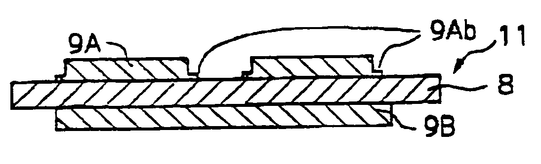
[0069]In steps A and B, a ceramic sheet 8 made of 96% pure alumina and which had a thickness of 0.25 mm was united by direct joining to aluminum sheets 9A and 9B on both principal surfaces, thereby preparing a composite member 7. In step C, an etching resist 10 was applied to the side of the composite member 7 where a circuit pattern was to be formed. Subsequently, in step D, the composite member 7 was mounted on the milling cutter and the unwanted areas of the aluminum layer 9A were removed by cutting with an end mill having a diameter of 1 mm such that a residual aluminum layer 9Aa would be left intact in a thickness of 50 μm. Thereafter, in step E, etching was performed to remove the remaining aluminum layer 9Aa. In subsequent step F, an end mill having a larger diameter of 1.2 mm w...
example 3
[0072]An aluminum-ceramic composite member was coated with an etching resist and milled with an end mill having a diameter of 1 mm as in Example 1. The composite member was prepared by direct joining of a 0.25-mm thick alumina sheet with two 0.4-mm thick aluminum sheets, one for providing a circuit and the other for a heat sink, in which the assembly was heated and then cooled down in an inert gas atmosphere.
[0073]The composite member was milled with a milling machine according to the circuit diagram shown in FIG. 4 under various conditions including rpm, cutting speed and time, thereby making eight samples of circuit board 14 each having a circuit made of an aluminum layer 13 on a ceramic substrate 12. The milling conditions and the results obtained are shown in Table 1 for the respective sample Nos. 1-8.
[0074]Sample Nos. 1 and 3 were measured for the dimensional precision of slit width (inter-element spacing) at 9 locations and the results were satisfactory as shown in Table 2.
[00...
PUM
 Abstract
Description
Claims
Application Information
 - R&D
- Intellectual Property
- Life Sciences
- Materials
- Tech Scout
- Unparalleled Data Quality
- Higher Quality Content
- 60% Fewer Hallucinations
Browse by: Latest US Patents, China's latest patents, Technical Efficacy Thesaurus, Application Domain, Technology Topic, Popular Technical Reports.
© 2025 PatSnap. All rights reserved.Legal|Privacy policy|Modern Slavery Act Transparency Statement|Sitemap|About US| Contact US: help@patsnap.com