Probe structure having a plurality of discrete insulated probe tips projecting from a support surface, apparatus for use thereof and methods of fabrication thereof

a technology of discrete insulated elongated electrical conductors and probe structures, which is applied in the direction of solid-state devices, semiconductor/solid-state device details, instruments, etc., can solve the problems of relatively expensive fabrication of contemporary probes for testing integrated circuits, and easy deformation or damage of probe wires. , to achieve the effect of reducing the length of electrical conductors

Inactive Publication Date: 2008-05-06
GLOBALFOUNDRIES INC
View PDF28 Cites 34 Cited by
  • Summary
  • Abstract
  • Description
  • Claims
  • Application Information

AI Technical Summary

Benefits of technology

[0017]Another object of the present invention is to provide a probe structure that is an integral part of the fan out wiring on the test...

Problems solved by technology

If the integrated circuit device is defective, the device and the plastic leaded chip carrier are discarded.
The semi-permanent attachment techniques used for testing integrated circuit devices such as solder ball attachment to a ceramic or plastic pin grid array package are typically used for devices that have high number of interconnections and the pin grid array package is relatively expensive.
If the integrated circuit device is defective, the device can be removed from the pin grid array package by heating the solder balls to their melting point.
Contemporary probes for testing integrated circuits are expensive to fabricate and are easily damaged.
The probe wires are generally fragile and easily deformed or damaged.
This type of probe is also much larger than the IC device that is being tested and the use of this type of probe for high temperature testing is limited by the probe structure and material set.
This type of probe is limited to flexible film substrate materials that typically have...

Method used


Image

  • Probe structure having a plurality of discrete insulated probe tips projecting from a support surface, apparatus for use thereof and methods of fabrication thereof
  • Probe structure having a plurality of discrete insulated probe tips projecting from a support surface, apparatus for use thereof and methods of fabrication thereof
  • Probe structure having a plurality of discrete insulated probe tips projecting from a support surface, apparatus for use thereof and methods of fabrication thereof

Examples


Embodiment Construction

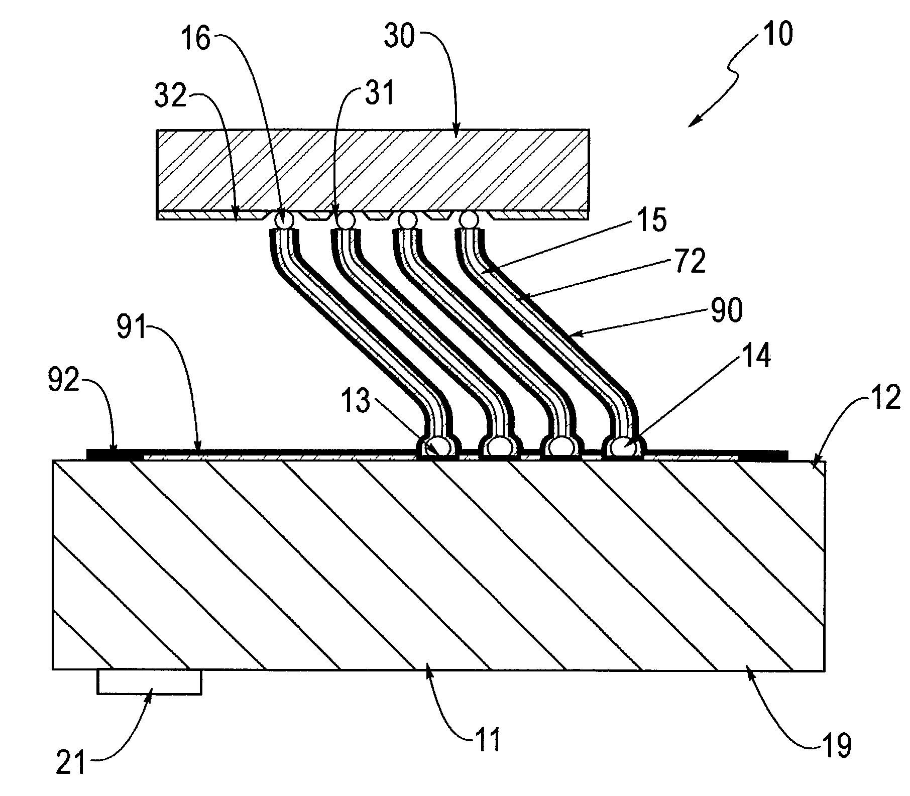
[0041]FIG. 1 shows a cross section of a test substrate (11) and a high performance test probe (10) according to the present invention. The test substrate (11) provides a rigid base for attachment of the probes (10) and fan out wiring from the high density array of probe contacts to a larger grid of pins or other interconnection means to the equipment used to electrically test the integrated circuit device. The fan out substrate can be made from various materials and constructions including single and multi-layer ceramic with thick or thin film wiring, silicon wafer with thin film wiring, and epoxy glass laminate construction with high density copper wiring. The test probes (10) are attached to the first surface (12) of the substrate (11). The probes are used to electrically contact the aluminum bond pads (31) on the device (30) which is being tested. The device (30) under test, is preferably an IC chip. The bond pads (31) which are typically aluminum are typically recessed slightly ...


PUM


Abstract

The present invention is directed to structures having a plurality of discrete insulated elongated electrical conductors projecting from a support surface which are useful as probes for testing of electrical interconnections to electronic devices, such as integrated circuit devices and other electronic components and particularly for testing of integrated circuit devices with rigid interconnection pads and multi-chip module packages with high density interconnection pads and the apparatus for use thereof and to methods of fabrication thereof. Coaxial probe structures are fabricated by the methods described providing a high density coaxial probe.

Description

[0001]This application is a continuation of Ser. No. 09 / 254,798, filed on Mar. 11, 1999, now U.S. Pat. No. 6,452,406, which is a 371 of PCT / US97 / 13698, filed on Sep. 12, 1997, which claims benefit of 60 / 026,050, filed Sep. 13, 1996. This application Ser. No. 10 / 202,069 is a CIP of Ser. No. 09 / 921,867, filed Aug. 3, 2001, now pending, which is a Continuation of Ser. No. 08 / 872,519 filed on Jun. 11, 1997, now U.S. Pat. No. 6,334,247 on Jan. 1, 2002, which is a Division of Ser. No. 08 / 754,869,filed on Nov. 22, 1996, now U.S. Pat No. 5,821,763 on Oct. 13, 1998, which is a Continuation of Ser. No. 08 / 055,485, filed on Apr. 30, 1993, now U.S. Pat. No. 5,635,846 on Jun. 3, 1997.CROSS REFERENCE TO RELATED APPLICATION[0002]The teaching of U.S. application Ser. No. 09 / 254,768, filed on the same day herewith entitled, “INTEGRATED COMPLIANT PROBE FOR WAFER LEVEL TEST AND BURNIN” to Brian S. Beaman et al., now U.S. Pat. No. 6,528,984 and the teaching of U.S. application Ser. No. 09 / 254,769 filed...

Claims


Application Information

Patent Timeline
IPC IPC(8): G01R31/02G01R1/067G01R1/073G01R3/00
CPCG01R1/0675G01R1/07307G01R1/07342G01R1/07371G01R3/00G01R31/2886H01L23/49827H01L23/5384H01L25/0652G01R1/06711H01L2924/10253H01L2924/00013H01L2224/13099G01R1/06772G01R1/07378H01L2224/1134H01L2224/16H01L2224/78301H01L2924/01014H01L2924/01046H01L2924/01078H01L2924/01079H01L2924/09701H01L2924/3011H01L2924/00H01L2924/1627H01L2924/00014H01L2224/0401
Inventor BEAMAN, BRIAN SAMUELFOGEL, KEITH EDWARDLAURO, PAUL ALFREDLIAO, YUN-HSINMORRIS, DANIEL PETERSHIH, DA-YUAN
Owner GLOBALFOUNDRIES INC
Why Eureka
Try Eureka