Apparatus and method for an improved lens structure for polymer wave guides which maximizes free space light coupling

a polymer waveguide and free space technology, applied in the field of polymer waveguides, can solve the problems of reducing the life of the battery in the device, obscuring the viewing of the underlying display, and reducing so as to reduce the sensitivity of optical coupling efficiency, improve optical coupling, and minimize problems

Inactive Publication Date: 2008-05-06
POA SANA LIQUIDATING TRUST
View PDF40 Cites 62 Cited by
  • Summary
  • Abstract
  • Description
  • Claims
  • Application Information

AI Technical Summary

Benefits of technology

[0014]The present invention is directed a polymer waveguide assembly. The waveguide assembly includes a polymer waveguide have a plurality of waveguide cores and an associated plurality of lenses respectively. The assembly also includes a molded lens structure having a support region, a primary refractive surface and a secondary refractive lens. The polymer waveguide is positioned onto the support surface of the molded lens structure so that the waveguide lenses are in optical alignment with the primary refractive lens and the secondary refractive lens of the molded waveguide structure. The lenses of the polymer waveguide are capable of collimating in the X and Y directions respectively. The primary refractive lens and the secondary refractive lens are both capable of collimating light in the Z direction. With this arrangement, a substantial; portion of the light passing through the secondary lens toward the waveguide cores is within the acceptance angle of the plurality of waveguides lenses respectively. The secondary lens thus creates a shallow angle of convergence relative to the input of the plurality of lenses of the waveguide. As a result, light received in free space and exiting the two lenses is substantially within the acceptance angle of the waveguide, allowing a significantly lower sensitivity of optical coupling efficiency with waveguide alignment, thereby minimizing problems caused by misalignment and improving optical coupling.

Problems solved by technology

This approach has a number of problems.
Foremost, the film causes the display to appear dim and obscures viewing of the underlying display.
However, in the case of most portable devices, such as cell phones, personal digital assistants, and laptop computers, the added intensity requires additional power, reducing the life of the battery in the device.
The films are also easily damaged.
In addition, the cost of the film scales dramatically with the size of the screen.
With large screens, the cost is typically prohibitive.
This type of data input display, however, also has a number of problems.
The relatively large number of LEDs and photodiodes, and the need for precise alignment, make such displays complex, expensive, and difficult to manufacture.
Since it is difficult to fabricate a three dimensional polymer lens using photolithography, current polymer waveguides do an inadequate job in collimating light in the Z plane.
As a consequence, single lens optical waveguides have poor optical coupling in the Z plane.
Problems arise with the aforementioned arrangement due to alignment issues.
In other words, if the polymer waveguides are not precisely aligned with their respective vertical lenses, it may result in the loss of optical coupling between transmit and receive waveguides.
For example if there a misalignment issues on the receiving end, then it is likely that the focal point of the vertical lens will fall outside the lenses of the polymer waveguide.
As a general rule, a slight misalignment will often cause a rather dramatic loss of optical coupling or power at the receiving waveguide.

Method used


Image

  • Apparatus and method for an improved lens structure for polymer wave guides which maximizes free space light coupling
  • Apparatus and method for an improved lens structure for polymer wave guides which maximizes free space light coupling
  • Apparatus and method for an improved lens structure for polymer wave guides which maximizes free space light coupling

Examples


Embodiment Construction

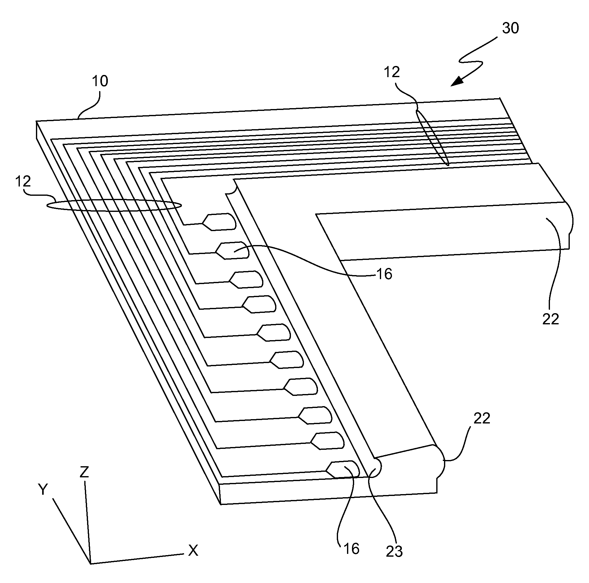
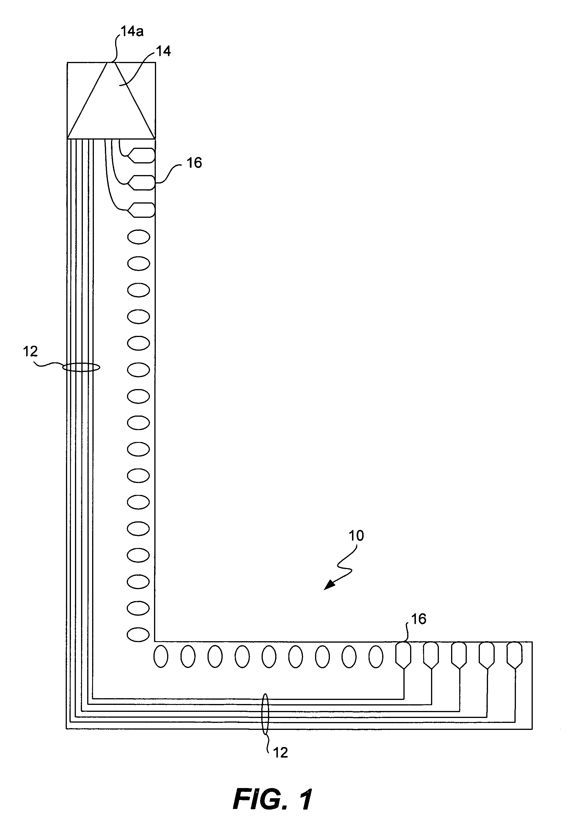
[0024]Referring to FIG. 1, a polymer waveguide 10 is shown. The waveguide 10 is an L-shaped member including a plurality of cores 12 that extend between an optical coupling end 14 of the waveguide 10 and a plurality of lenses 16 respectively (for the sake of simplicity, not all the cores 12 are illustrated). The optical coupling end 14 includes an expansion horn 14a, which, tapers to a single source. The individual lenses 16 are provided along the inner periphery of the waveguide 10. Each of the lenses 16 is optically coupled to one of the cores 12 which runs the length of the waveguide 10 and terminates at the optical coupling end 14.

[0025]In one embodiment, the polymer waveguide 10 is manufactured using photolithography. A first polymer cladding layer having an index of refraction N1 is formed on a substrate. A second polymer cladding layer, having an index of refraction N2, which is greater than N1, is formed over the first layer. The second polymer layer is patterned to form the...


PUM


Abstract

A polymer waveguide assembly. The assembly includes a polymer waveguide have a plurality of waveguide cores and an associated plurality of lenses respectively. The assembly also includes a molded lens structure having a support region, a primary refractive surface and a secondary refractive lens. The polymer waveguide is positioned onto the support surface of the molded lens structure so that the waveguide lenses are in optical alignment with the primary refractive lens and the secondary refractive lens of the molded waveguide structure. The lenses of the polymer waveguide are capable of collimating in the X and Y directions respectively. The primary refractive lens and the secondary refractive lens are both capable of collimating light in the Z direction. With this arrangement, a substantial; portion of the light passing through the secondary lens toward the waveguide cores is within the acceptance angle of the plurality of waveguides lenses respectively. The secondary lens thus creates a shallow angle of convergence relative to the input of the plurality of lenses of the waveguide. As a result, issues caused by misalignment are minimized and optical coupling is improved.

Description

BACKGROUND OF THE INVENTION[0001]1. Field of the Invention[0002]The present invention relates generally to polymer waveguides used for light generation and reception in touch screen displays, and more particularly, to an improved lens structure for free space optical systems which maximizes the free space light coupling between transmit and receive waveguides.[0003]2. Description of the Related Art[0004]User input devices for data processing systems can take many forms. Two types of relevance are touch screens and pen-based screens. With either a touch screen or a pen-based screen, a user may input data by touching the display screen with either a finger or an input device such as a stylus or pen.[0005]One conventional approach to providing a touch or pen-based input system is to overlay a resistive or capacitive film over the display screen. This approach has a number of problems. Foremost, the film causes the display to appear dim and obscures viewing of the underlying display. To...

Claims


Application Information

Patent Timeline
Patent Type & Authority Patents(United States)
IPC IPC(8): G02B6/32G02B6/26G02B6/42G06F3/042
CPCG02B6/12004G02B6/1221G02B6/1228G02B6/32G06F3/0421
Inventor DEANE, PETER
Owner POA SANA LIQUIDATING TRUST
Why Eureka
Try Eureka