Gallium nitride compound semiconductor device and manufacturing method

a technology of gallium nitride and semiconductor devices, which is applied in the direction of semiconductor devices, electrical devices, nanotechnology, etc., can solve the problems of insufficient capture of carriers, insufficient efficiency reduction, and labor-intensive manufacturing, and achieve the effect of superior light emission efficiency

Active Publication Date: 2008-05-13
NITRIDE SEMICON
View PDF12 Cites 69 Cited by
  • Summary
  • Abstract
  • Description
  • Claims
  • Application Information

AI Technical Summary

Benefits of technology

[0006]An object of the present invention is to provide a device having a superior light emission efficiency in a short wavelength range (in particular, in a wavelength range of 400 nm or shorter) without using a special method such as photolithography.
[0021]According to another aspect of the present invention, it is preferable that the gallium nitride-based compound semiconductor device further comprises an n electrode which is connected to the n-type GaN-based layer, a p electrode which is connected to the p-type GaN-based layer, and a power supply which applies a voltage between the n electrode and the p electrode. According to another aspect of the present invention, it is preferable that the gallium nitride-based compound semiconductor device is used as a light source to realize a device which irradiates light having a wavelength of 400 nm or shorter. Because a device in which the gallium nitride-based compound semiconductor device according to the present invention is incorporated as a light source has a superior light emission efficiency at a short wavelength band (wavelength of 400 nm or shorter), such a device is applicable for uses which require a light source of a short wavelength.

Problems solved by technology

As a consequence, the carriers do not reach the dislocations and the efficiency is not reduced.
When the fluctuation in composition is small, the carriers are not sufficiently captured.
However, because these methods require photolithography or the like, there had been a problem in that the manufacturing requires labor and the cost of the light emitting element is increased.

Method used


Image

  • Gallium nitride compound semiconductor device and manufacturing method
  • Gallium nitride compound semiconductor device and manufacturing method
  • Gallium nitride compound semiconductor device and manufacturing method

Examples


first preferred embodiment

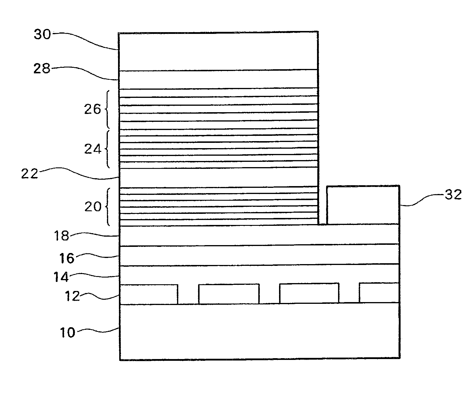
[0026]FIG. 1 shows a structure of a light emitting element (LED) which is a GaN-based compound semiconductor according to a first preferred embodiment of the present invention. The light emitting element is manufactured by growing a plurality of layers on a substrate through an MOCVD method (Metal Organic Chemical Vapor Deposition). More specifically, the light emitting element is manufactured through the following processes. First, an MOCVD device will be briefly described, although the MOCVD device itself is well known in the art. A susceptor and a gas introduction tube are provided within a reaction tube. A substrate is placed on the susceptor and a material gas is supplied while the substrate is heated by a heater to let a reaction occur on the substrate. The gas introduction section is provided, for example, at two locations of the reaction tube. A material gas such as trimethyl gallium and silane gas is introduced from one location from a lateral direction of the substrate and...

second preferred embodiment

[0067]When texts, objects, or the like are drawn by a commercially available black pen (fluorescent pen), the drawn objects cannot be seen under visible light illumination, but can be seen when an ultraviolet ray is irradiated onto the drawn objects. Although a color black pen (a color object appears when ultraviolet ray is irradiated) is also commercially available, in order to reproduce colors, the wavelength of the ultraviolet ray to be irradiated must be 400 nm or shorter, more precisely, 380 nm or shorter. In the related art, a light source such as a fluorescence black light or a mercury lamp is used. However, these light sources are large and consume large power and there is a problem in that a large-scale power supply is necessary.

[0068]When the light emitting element device (LED) as shown in FIG. 1 is used as a light source for reproducing the drawn objects, the device is small and can be driven by a battery. Objects drawn by a black pen were reproduced by irradiating light ...

third preferred embodiment

[0071]The LED according to the present embodiment was irradiated onto the skin of a human body for a short period of time and the effects of the irradiation were observed. Light was irradiated from LEDs having peak wavelengths of 400 nm (5 mW), 385 nm (3 mW), and 372 nm (1 mW) onto the skin for 10 minutes and changes in the skin (commonly referred to as “tanning”) were observed. As a result, it was found that in the case of the LED of peak wavelength of 400 nm (5 mW), there was almost no effect while there was some change in the case of the LED of 385 nm (3 mW). In the case of the LED of 372 nm (1 mW), on the other hand, there was significant tanning. These results show that the LED in the wavelength band of 365 nm-380 nm causes tanning of the human body. Tanning devices were manufactured using the LED as a light source. A tanning device which allows tanning of a spot of a diameter of 5 mm and a tanning device in which LEDs were placed on a straight line having a length of 3 cm to a...


PUM


Abstract

A light-emitting element using GaN. On a substrate (10), formed are an SiN buffer layer (12), a GaN buffer layer (14), an undoped GaN layer (16), an Si-doped n-GaN layer (18), an SLS layer (20), an undoped GaN layer (22), an MQW light-emitting layer (24), an SLS layer (26), and a p-GaN layer (28), forming a p electrode (30) and an n electrode (32). The MQW light-emitting layer (24) has a structure in which InGaN well layers and AlGaN barrier layers are alternated. The Al content ratios of the SLS layers (20, and 26) are more than 5% and less than 24%. The In content ratio of the well layer in the MQW light-emitting layer (24) is more than 3% and less than 20%. The Al content ratio of the barrier layer is more than 1% and less than 30%. By adjusting the content ratio and film thickness of each layer to a desired value, the light luminous efficiency for wavelength of less than 400 nm is improved.

Description

TECHNICAL FIELD[0001]The present invention relates to a gallium nitride (GaN)-based compound semiconductor device and a manufacturing method thereof, and, in particular, to improvement in light emission efficiency.BACKGROUND ART[0002]Light emitting elements which use a nitride semiconductor and have a wavelength band of 370 nm-550 nm have been made commercially available. In these light emitting elements, InxGa1-xN (0<x<1) is used as a light emitting material. The light emission wavelength changes when a compositional ratio of In in InxGa1-xN is changed. Specifically, the light emission wavelength is increased as x is increased. When the compositional ratio x of In is changed, the light emission efficiency also changes in addition to the light emission wavelength. More specifically, when the compositional ratio x of In is increased too much, because (1) a difference in lattice constants between InGaN and the layers sandwiching InGaN, that is, between InGaN and GaN or between I...

Claims


Application Information

Patent Timeline
Patent Type & Authority Patents(United States)
IPC IPC(8): H01L29/06H01L33/04H01L33/06H01L33/32
CPCB82Y20/00H01L33/32H01L33/04H01L33/06
Inventor SATO, HISAOSUGAHARA, TOMOYAKITAZAWA, SHINJIMURAMOTO, YOSHIHIKOSAKAI, SHIRO
Owner NITRIDE SEMICON
Why Eureka
Try Eureka