Voltage level conversion circuit

a voltage level conversion and circuit technology, applied in electronic switching, pulse automatic control, pulse technique, etc., can solve the problems of preventing circuit breakage and impeded power consumption reduction, so as to speed up the operation speed of the voltage level conversion circuit as a whole, suppress the driving ability of transistors, and speed up the effect of level converter

Active Publication Date: 2008-05-13
PANASONIC SEMICON SOLUTIONS CO LTD
View PDF7 Cites 9 Cited by
  • Summary
  • Abstract
  • Description
  • Claims
  • Application Information

AI Technical Summary

Benefits of technology

[0027]According to a first aspect of the present invention, there is provided a voltage level conversion circuit for converting an input signal having a logical voltage level corresponding to a first power supply voltage into an output signal having a logical voltage level corresponding to a second power supply voltage that is lower than the first power supply voltage, wherein a first P channel MOS transistor having the second power supply voltage as a breakdown voltage and a first N channel MOS transistor having the first power supply voltage as a breakdown voltage are connected in series between the second power supply voltage and a ground voltage; a second P channel MOS transistor having the second power supply voltage as a breakdown voltage and a second N channel MOS transistor having the first power supply voltage as a breakdown voltage are connected in series between the second power supply voltage and the ground voltage; a first connection node of the first P channel MOS transistor and the first N channel MOS transistor is connected to a gate of the second P channel MOS transistor; a second connection node of the second P channel MOS transistor and the second N channel MOS transistor is connected to a gate of the first P channel MOS transistor; and the output signal is supplied from the second connection node to a circuit that is driven by the second power supply voltage. In this first aspect, the voltage level conversion circuit for converting the logical voltage level of an input signal is provided with a level converter which is driven by a low power supply voltage and converts the input signal having a logical voltage level corresponding to a high power supply voltage into an output signal having a logical voltage level corresponding to the low power supply voltage, and the output signal which is obtained by level-shifting the input signal by the level converter is supplied to a circuit driven by the low power supply voltage. Therefore, transistors having breakdown voltages equal to the low power supply voltage can be used as the transistors constituting the circuit in the rear stage of the level converter. Thereby, it is possible to set the low power supply voltage of the level converter at a value lower than the threshold value of the transistor having a breakdown voltage equal to the high power supply voltage, resulting in a voltage level conversion circuit that can be operated by a lower internal voltage.
[0028]According to a second aspect of the present invention, in the voltage level conversion circuit according to the first aspect, the driving abilities of the first P channel MOS transistor and the second P channel MOS transistor are smaller than the driving abilities of the first N channel MOS transistor and the second N channel MOS transistor. In this second aspect, since the driving abilities of the first P channel MOS-transistor and the second P channel MOS transistor are set to values smaller than the driving abilities of the first N channel MOS transistor and the second N channel MOS transistor, it is possible to speed up the operation of the level converter when the N channel MOS transistors are in their on states.
[0029]According to a third aspect of the present invention, the voltage level conversion circuit according to the first aspect further includes a NOT circuit which is constituted by a third P channel MOS transistor having the second power supply voltage as a breakdown voltage and a third N channel MOS transistor having the second power supply voltage as a breakdown voltage, the driving ability of the third N channel MOS transistor being smaller than the driving ability of the third P channel MOS transistor, and the output signal is supplied through the NOT circuit to the circuit driven by the second power supply voltage. In this third aspect, there is provided the NOT circuit which is constituted by the third P channel MOS transistor and the third N channel MOS transistor having a driving ability lower than that of the third P channel MOS transistor, and the output signal is supplied through the NOT circuit to the circuit driven by the second power supply voltage. Therefore, the NOT circuit in the rear stage of the level converter can compensate for the driving ability of the N channel MOS transistor being lower than the driving ability of the P channel MOS transistor in the level converter, whereby the operation speed of the voltage level conversion circuit as a whole can be further increased.
[0030]According to a fourth aspect of the present invention, in the voltage level conversion circuit according to the first aspect, a first resistor is inserted between the first P channel MOS transistor and the first N channel MOS transistor; and a second resistor is inserted between the second P channel MOS transistor and the second N channel MOS transistor. In this fourth aspect, since the resistors are connected in series to the respective P channel MOS transistors constituting the level converter to suppress the driving abilities of transistors, the driving efficiencies of the N channel transistors constituting the level converter are substantially enhanced, whereby the operation of the level converter can be speeded up when the N channel MOS transistors are in their on states.
[0031]According to a fifth aspect of the present invention, the voltage level conversion circuit according to the first aspect comprises a fifth P channel MOS transistor connected between the first connection node and the second power supply voltage; a sixth P channel MOS transistor connected between the second connection node and the second power supply voltage; a first signal generation circuit for applying a one-shot pulse voltage for turning on the sixth P channel MOS transistor to a gate of the sixth P channel MOS transistor, when an L level logical voltage generated at the first connection node is detected; and a second signal generation circuit for applying a one-shot pulse voltage for turning on the fifth P channel MOS transistor to a gate of the fifth P channel MOS transistor, when an L level logical voltage generated at the second connection node is detected. In this fifth aspect, since there are provided the auxiliary P channel MOS transistors for supporting the operations of the P channel MOS transistors in the level converter and the auxiliary P channel MOS transistors are driven by the one-shot pulses, respectively, the voltage level conversion circuit can be operated at higher speed with more stability.

Problems solved by technology

In this case, however, the breakdown voltage of the transistors constituting the rear-stage NOT circuit 201b is lowered, which brings about the possibility of circuit breakage.
Therefore, the voltage level conversion circuit 201 impedes reduction in power consumption by low voltage driving and miniaturization of transistors in the semiconductor device.

Method used


Image

  • Voltage level conversion circuit
  • Voltage level conversion circuit
  • Voltage level conversion circuit

Examples


embodiment 1

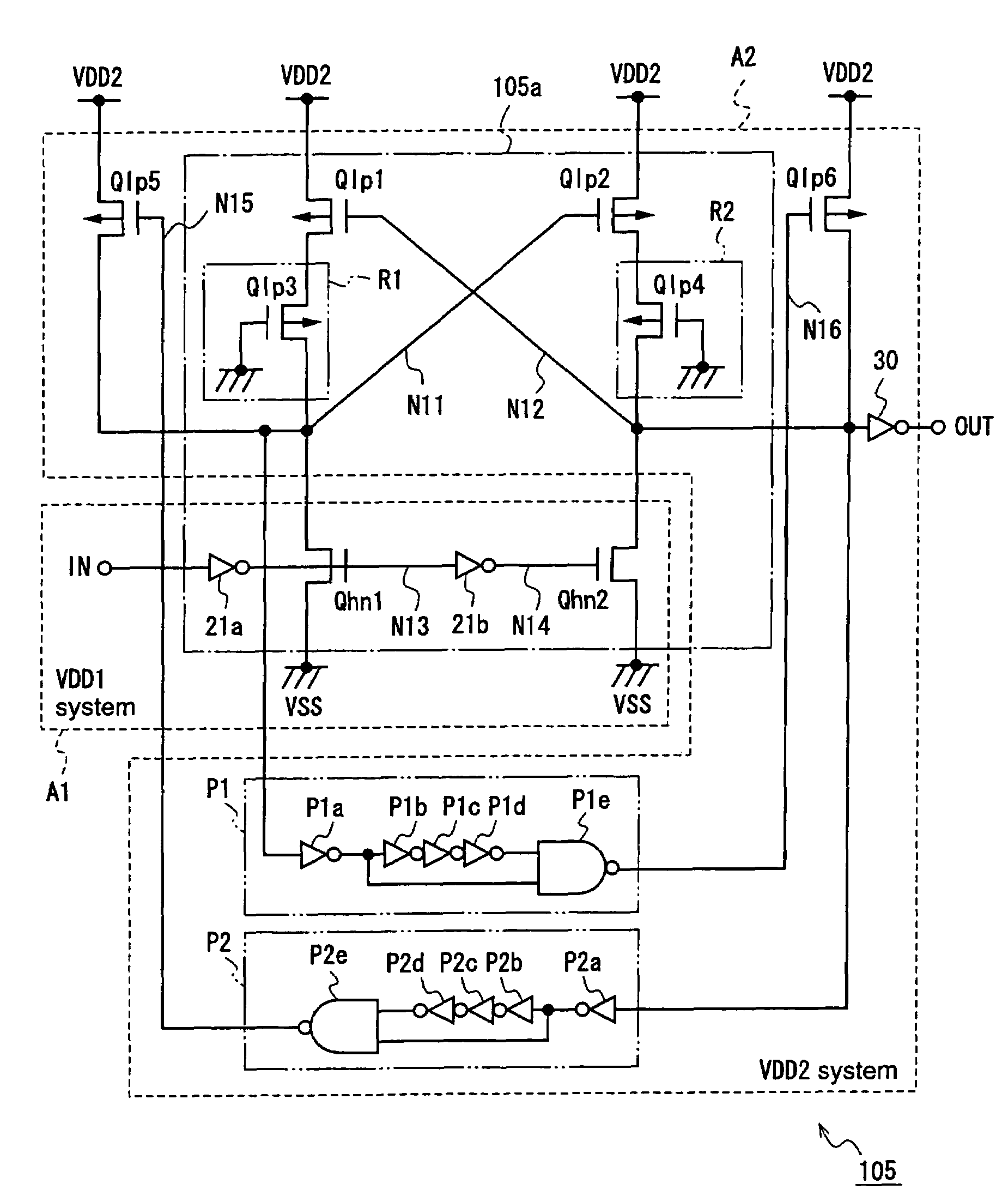
[0040]FIG. 1 is a circuit diagram for explaining a voltage level conversion circuit 101 according to a first embodiment of the present invention.

[0041]The voltage level conversion circuit 101 according to the first embodiment is a circuit for converting an input signal having a logical voltage level of a high power supply voltage system (VDD1 system) into an output signal having a logical voltage level of a low power supply voltage system (VDD2 system). The voltage level conversion circuit 101 includes a level converter which comprises a high breakdown voltage N channel MOS transistor and a low breakdown voltage P channel MOS transistor having a threshold value lower than that of the N channel MOS transistor, wherein the VDD1 system input signal is input to only the gate of the high breakdown voltage N channel MOS transistor, and the level converter outputs the input signal that is level-converted by the level converter to a circuit that is driven by the low power supply voltage, wh...

embodiment 2

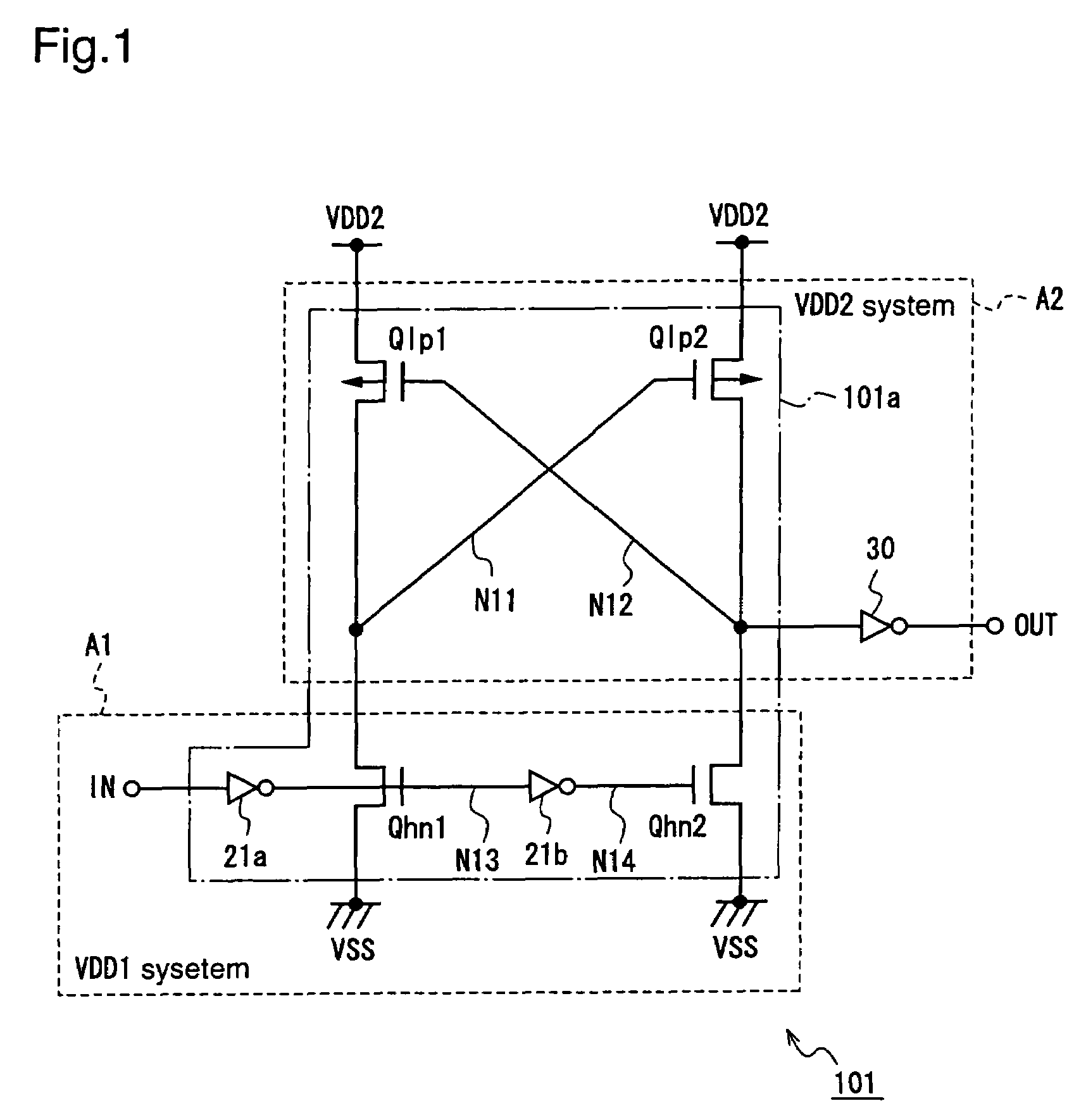
[0052]FIG. 2 is a circuit diagram for explaining a voltage level conversion circuit according to a second embodiment of the present invention.

[0053]A voltage level conversion circuit 102 according to the second embodiment is provided with, instead of the NOT circuit 30 of the voltage level conversion circuit according to the first embodiment, a NOT circuit 31 for adjusting the balance of transistor performance in a level converter 101a, and an output signal from the NOT circuit 31 is output through an output circuit 41 for waveform shaping.

[0054]In FIG. 2, the voltage level conversion circuit 102 includes a level converter 101a of the same construction as that according to the first embodiment, a NOT circuit 31 for inverting a signal outputted from the level converter 101a, and an output circuit 41 for shaping the waveform of a NOT signal outputted from the NOT circuit 31 and outputting the signal. The NOT circuit 31 comprises a third P channel MOS transistor Qlp7 and a third N chan...

embodiment 3

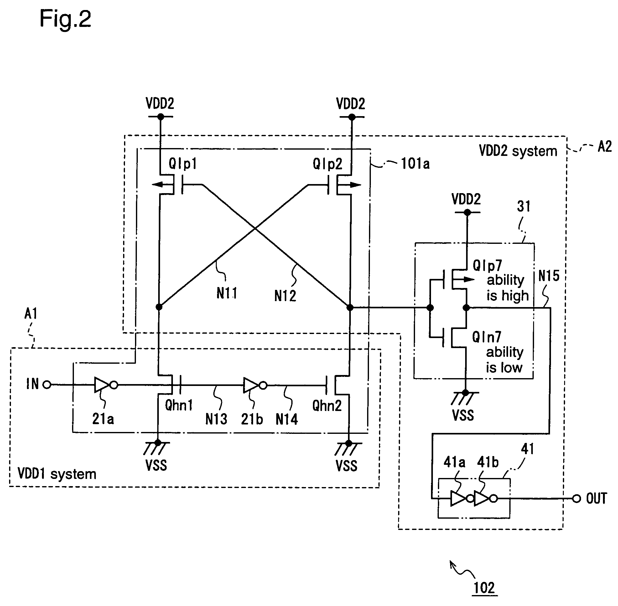
[0063]FIG. 3 is a circuit diagram for explaining a voltage level conversion circuit according to a third embodiment of the present invention.

[0064]A voltage level conversion circuit 103 according to the third embodiment is provided with a level converter 103a instead of the level converter 101a of the voltage level conversion circuit according to the first embodiment.

[0065]The level converter 103a of the voltage level conversion circuit according to the third embodiment is constructed by inserting a resistor R1 between the first connection node N11 and the first P channel MOS transistor Qlp1 in the level converter 101a according to the first embodiment, and inserting a resistor R2 between the second connection node N12 and the second P channel MOS transistor Qlp2 in the level converter 101a.

[0066]The resistor R1 comprises a P channel MOS transistor Qlp3 which is connected in series between the first connection node N11 and the first P channel MOS transistor Qlp1, and has a gate con...


PUM


Abstract

A voltage level conversion circuit is provided with a level converter for converting a VDD1 system input signal into a VDD2 system signal, and a NOT circuit for inverting the level-converted input signal and outputting the inverted signal, and the outputs of VDD1 system NOT circuits constituting the level converter are input to only high breakdown voltage transistors in the level converter while a signal having a logical voltage level corresponding to the low power supply voltage VDD2 is input to low breakdown voltage transistors, and further, only the input signal level-converted by the level converter is input to the NOT circuit.

Description

FIELD OF THE INVENTION[0001]The present invention relates to a voltage level conversion circuit and, more particularly, to a voltage level conversion circuit for converting an input signal having a logical voltage level corresponding to a first power supply voltage into an output signal having a logical voltage level corresponding to a second power supply voltage that is lower than the first power supply voltage.BACKGROUND OF THE INVENTION[0002]In recent years, with miniaturization of semiconductor devices, two kinds of voltages, i.e., an external voltage and an internal voltage, are used and the internal voltage is set lower than the external voltage. Therefore, there is a request for a circuit for converting the logical voltage level of a signal between a circuit driven by the external voltage and a circuit driven by the internal voltage.[0003]Hereinafter, a description will be given of prior arts with respect to a circuit for converting a logical voltage level corresponding to a ...

Claims


Application Information

Patent Timeline
Patent Type & Authority Patents(United States)
IPC IPC(8): H03L5/00H03K19/0185H03K3/012H03K3/356H03K17/10
CPCH03K3/012H03K3/356113H03K3/356165H03K17/102
Inventor HIRANO, HIROSHIGE
Owner PANASONIC SEMICON SOLUTIONS CO LTD
Why Eureka
Try Eureka