Method for producing self-aligned mask, articles produced by same and composition for same

a mask and self-aligning technology, applied in the field of patterns, can solve the problems of reducing and accelerating the passage of interconnect signals, so as to reduce the electromigration attributes of metal lines, maximize the propagation speed of interconnect signals, and reduce the effective dielectric constant of interconnect structures.

Inactive Publication Date: 2008-05-27
TAIWAN SEMICON MFG CO LTD
View PDF4 Cites 13 Cited by
  • Summary
  • Abstract
  • Description
  • Claims
  • Application Information

AI Technical Summary

Benefits of technology

[0006]Consequently, the pattern generated in the masking material is self-aligned to the substrate upon which it is placed. The method of the present invention can apply to any technology or application involving a heterogeneous substrate including, for example, interconnect structures for high speed microprocessors, application specific integrated circuits (ASICs), memory storage, displays, hi-throughput screening methods, such as a lab on a chip, microfabricated fluidic devices, etc. The utility of the inventive method stems from a simple and robust means in which the replication of a patterned substrate to generate a self-aligned mask can be performed, circumventing the requirement for difficult and error prone methods, such as alignment of a lithography mask relative to pre-patterned substrate.
[0007]Thus, the present invention provides an extremely advantageous alternative to the prior art techniques. The present invention provides a means to replicate a pattern on a pre-patterned substrate in such as manner as to act as a mask. For example, the effective dielectric constant of an interconnect structure can be reduced by the use of a process where layers are selectively placed upon a capped interconnect structure and used to remove the high-k dielectric cap between the metal lines. Additionally, in the opposite tone, for which self-alignment is on the dielectric / hard-mask surfaces of an interconnect structure, the resist, can then be used as a mask for subsequent deposition of other layers that serve as diffusion barriers to copper, barriers to oxygen and / or water permeation, layers which reduce the electromigration attributes of the metal lines, and seed layers. By using these processes, the mask can be self-aligned such that overlay processes are not required to define the features. Both tones of masking (i.e., positive and negative) can be beneficial depending on subsequent processing requirements. An additional benefit of the present invention is that neither an expensive lithography mask, nor an expensive lithography system is required. Rather, a simple exposure tool that is able to generate a blanket exposure can be utilized. In some embodiments of the present invention, it may be beneficial to have an exposure system that is monochromatic.
[0008]Thus, in the example of integrated circuits, the use of the self-aligned masks allows a unique process in which the effective dielectric constant between metal lines can be reduced through selective application of various materials to the metal lines or as a selective mask for removing high-k dielectric material between the metal lines. The term “high-k dielectric” is used in the present invention to denote an insulator material that has a dielectric constant, k, greater than 3.0 preferably greater than 7.0. This is of great importance in maximizing the propagation speed of interconnect signals and ultimately provides faster overall circuit performance. Furthermore, the present invention leads to a higher level of protection as well as reliability of interconnect structures and reduced processing costs relative to comparable lithographic processes utilizing overlay strategies.
[0013]In one embodiment, the developed patterned masking material may be exposed to a dry etch process to expose either a first region or a second region on the substrate. In another embodiment, the masking material has a thickness equal to a minima or maxima in a plot of reflectivity versus resist film thickness for one or more of the surfaces of interest. In yet another embodiment of the present invention, the masking material has a thickness that maximizes the difference in the thickness of the masking material in a plot of film thickness versus exposure dose for one or more of the surfaces of interest. In that embodiment of the present invention, the masking material may have a thickness of zero over one or more of the surfaces of interest.

Problems solved by technology

Unfortunately, typical procedures used to generate a mask by lithographic or other means can be expensive and error prone, particularly when alignment or overlay is required.
Both of these approaches reduce the effective dielectric constant, keff, of the components between metal lines and as a result, interconnect signals travel faster through conductors due to a reduction in resistance-capacitance (RC) delays.
Unfortunately, these strategies are difficult to implement due to limitations in maintaining sufficient properties, i.e., mechanical, barrier, electrical, etc., that result when there is a reduction in thickness or changes in the chemistry of the layers.

Method used


Image

  • Method for producing self-aligned mask, articles produced by same and composition for same
  • Method for producing self-aligned mask, articles produced by same and composition for same
  • Method for producing self-aligned mask, articles produced by same and composition for same

Examples


Embodiment Construction

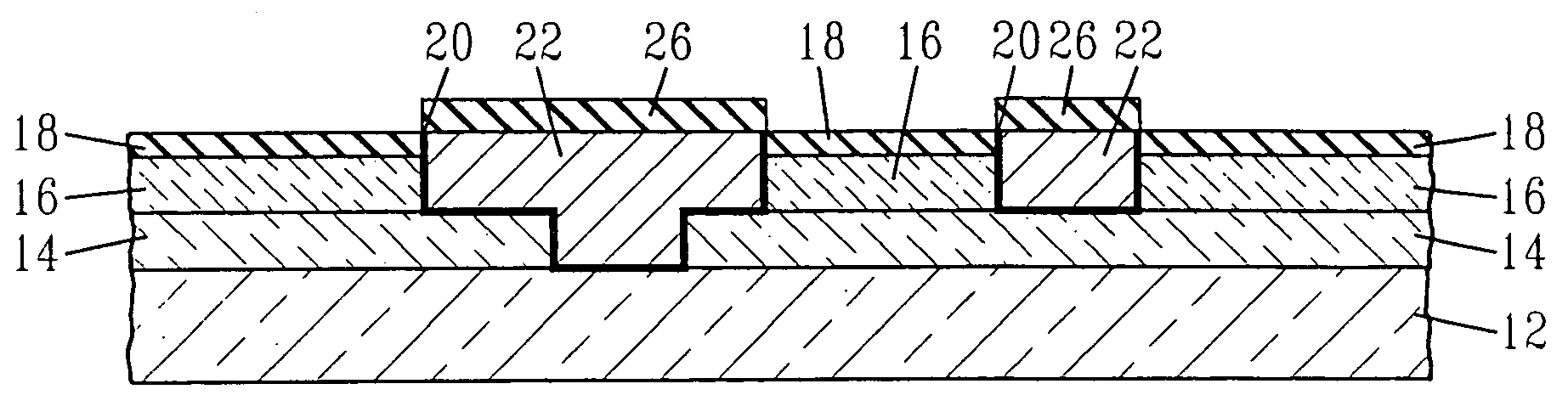
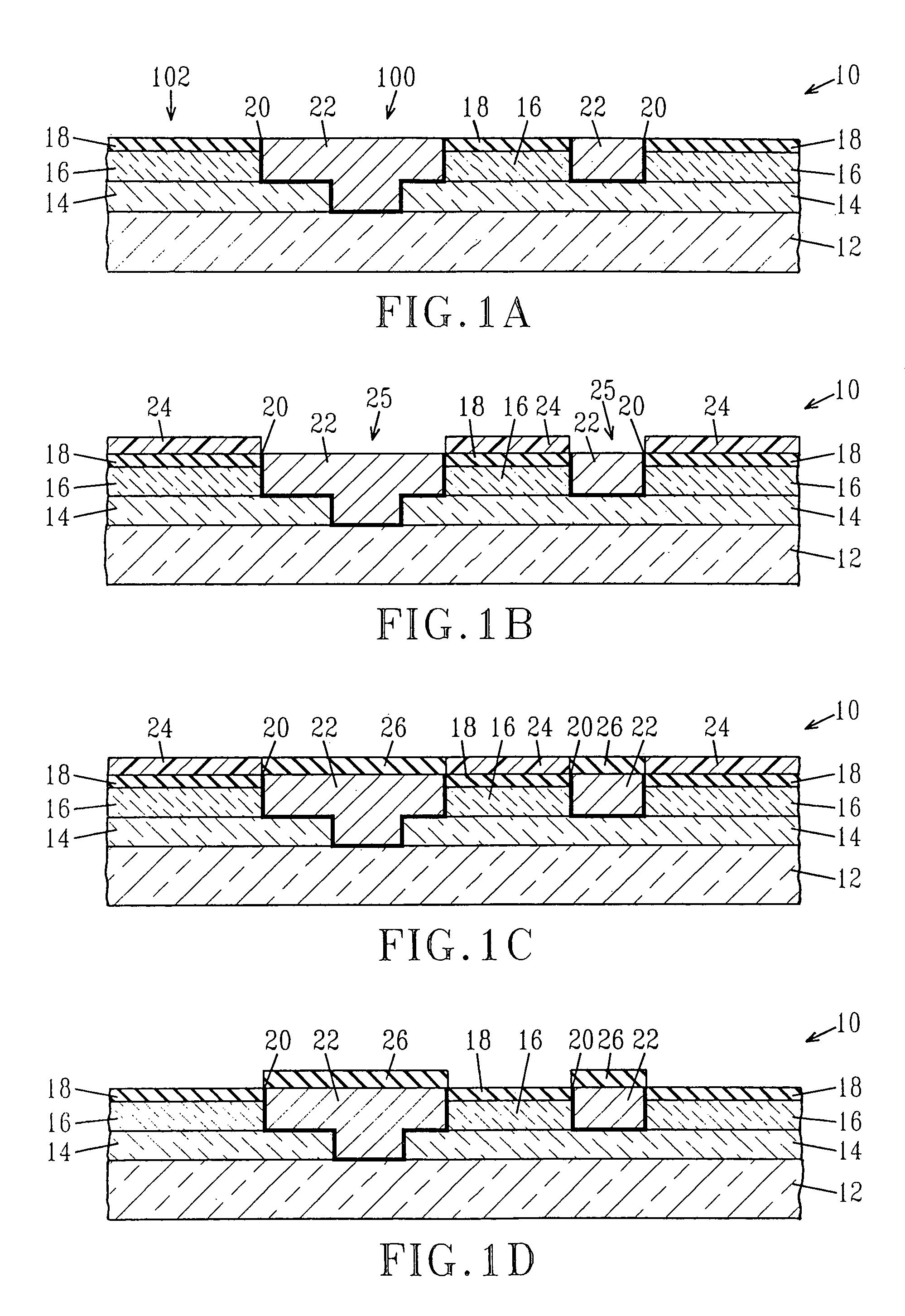
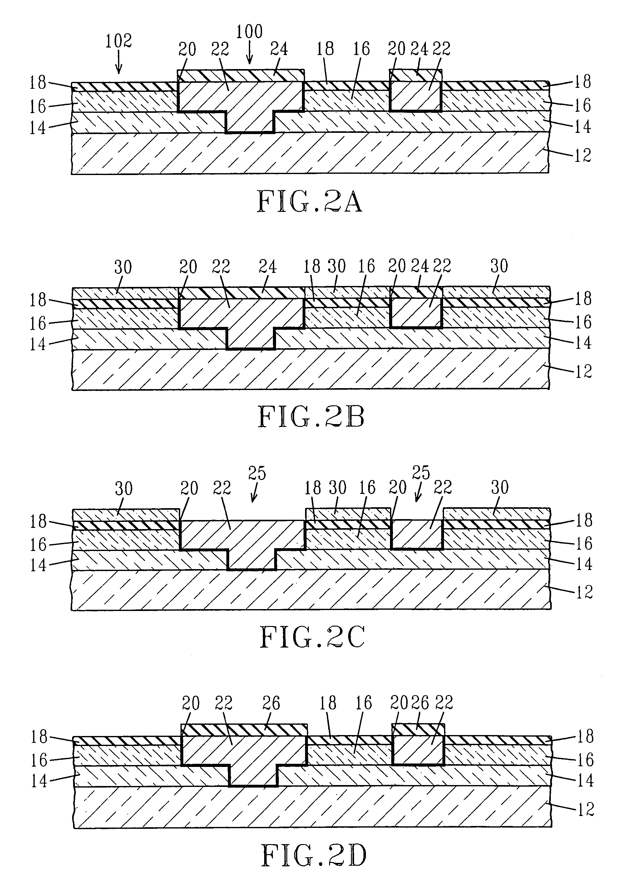
[0027]As stated above, the present invention provides a patterned substrate containing structures having two or more distinct components processed by a route whereby masking layers can be applied to selected component surfaces. These masking layers can be generated by a number of self-assembly approaches described below and can be used as a mask for subsequent treatment or material deposition onto the intended component surfaces. These structures can be sacrificial and, in general, do not remain in the final structure.

[0028]The use of masks for the generation of self assembled barrier layers can proceed by a number of different routes including: blanket deposition, followed by lift-off, blanket deposition followed by chemical mechanical polishing (CMP), and enhancement of selective electrochemical and electroless metal deposition processes. It will be clear to one skilled in the art that the application of a self-aligned masking layer by any of the approaches described herein can be...


PUM

PropertyMeasurementUnit
dielectric constantaaaaaaaaaa
wavelengthaaaaaaaaaa

Abstract

A method for forming a self-aligned pattern on an existing pattern on a substrate comprising applying a coating of a solution containing a masking material in a carrier, the masking material being either photo or thermally sensitive; performing a blanket exposure of the substrate; and allowing at least a portion of the masking material to preferential develop in a fashion that is replicates the existing pattern of the substrate. The existing pattern may be comprised of a first set of regions of the substrate having a first reflectivity and a second set of regions of the substrate having a second reflectivity different from the first composition. The first set of regions may include one or more metal elements and the second set of regions may include a dielectric. Structures made in accordance with the method.

Description

FIELD OF THE INVENTION[0001]The present invention relates to the production of patterns on a substrate having regions with different optical properties, i.e., reflectivity, absorbance or transparency. More particularly, the present invention relates to a method of producing fine patterns on substrates used in, for example, the microelectronics industry on which electronic devices are fabricated. The present invention also relates to devices fabricated in accordance with the inventive method. The patterns are fabricated accurately and inexpensively without the use of typical lithography steps that include overlay of a mask pattern to a pre-patterned substrate. The present invention also provides many additional advantages, which shall become apparent as described below.BACKGROUND OF THE INVENTION[0002]A number of applications and technologies involve structures having a well-defined arrangement of distinct regions. Normally, these structures are defined by patterning processes such a...

Claims


Application Information

Patent Timeline
Patent Type & Authority Patents(United States)
IPC IPC(8): H01L23/48H01L23/52H01L29/40G03F7/00G03F7/20H01L23/58
CPCG03F7/0035G03F7/2051H01L21/76834H01L21/76849G03F7/2022Y10S430/146
Inventor BRUNNER, TIMOTHY A.COLBURN, MATTHEW E.HUANG, ELBERTSANKARAPANDIAN, MUTHUMANICKAM
Owner TAIWAN SEMICON MFG CO LTD
Why Eureka
Try Eureka