Method of connecting module layers suitable for the production of microstructure modules and a microstructure module

a technology of microstructure modules and layers, applied in the direction of microstructure technology, microstructure devices, microstructure components, etc., can solve the problems of insufficient cost-effectiveness and insufficient reliability of known manufacturing methods for microstructure components, and achieve low component offset, low cost, and sufficient flectional strength.

Inactive Publication Date: 2008-06-03
ATOTECH DEUT GMBH
View PDF52 Cites 15 Cited by
  • Summary
  • Abstract
  • Description
  • Claims
  • Application Information

AI Technical Summary

Benefits of technology

[0070]Placed on the bottom plate and used as pressure cushions are preferably high temperature-proof ceramic fiber papers as ceramic fleece in a thickness of approximately 1-10 mm, preferably 2-4 mm. This compensates a potential difference in height between the components and provides uniform pressure distribution. Then an intermediate plate, preferably made of graphite, ceramic, steel, or composite, that has sufficient flectional strength, pressure stability, and heat conductivity, in a thickness of 1-30 mm, preferably 10-20 mm, is placed on the ceramic fiber paper in order to prevent it from bonding to the metal components. The components layers are stacked on the intermediate plate, either individually or preferably in multiple panels. If films of multiple components are to be joined at the same time stacked individually or in multiple panels, the films are separated from one another for instance by graphite intermediate layers.
[0071]In the case of joining individual stacks, the offset of the individual films is minimized by the use of special registration apparatus, registration pins, or templates. The registration apparatus, registration pins, or templates preferably comprise a material selected from the group including graphite, ceramic, and metal, the surface of which is coated with an appropriate protective coating, preferably a protective ceramic coating. The height of the registration apparatus, registration pins, or templates should be lower than the stack of films. However, it is also possible to provide corresponding depressions in the base plate and cover plate, which can then offer the advantage of registration on both sides (from above and below). When using multiple panels, preferably metal or non-metal registration pins can be used. For this purpose, provided in the structuring process in the edge area of the panel are corresponding recesses into which registration pins can be inserted so that a low offset in the components can be assured with minimum tolerance. Also, the registration pins preferably are lower in height than the entire component. However, the panels can also have structural features, preferably in the edge area of the component layers, that facilitate auto-registration, e.g., stamped, etched, or punched depressions that prevent the individual layers from being offset when stacked. After the soldering / brazing process, the component layers are detached from the multiple panels, e.g., by cutting, milling, punching, lasering. Placed on the panels or on the films stacked in the registration apparatus is a graphite platter and ceramic fiber paper that form the closure to the upper pressure plate.

Problems solved by technology

Thus, the problem upon which the present invention is based is that known manufacturing methods for microstructure components are not sufficiently reliable to ensure that the pressure resistance and corrosion resistance of the component is high enough that the component's tightness against fluid exiting from the component or fluid spilling over into adjacent microchannels is high enough and that the microchannels have a sufficiently low flow resistance.
In addition, known manufacturing methods are not cost-effective enough that the microstructured components can be employed in a wide variety of applications.

Method used


Image

  • Method of connecting module layers suitable for the production of microstructure modules and a microstructure module
  • Method of connecting module layers suitable for the production of microstructure modules and a microstructure module
  • Method of connecting module layers suitable for the production of microstructure modules and a microstructure module

Examples


Embodiment Construction

[0146]The invention is explained in greater detail in the following.

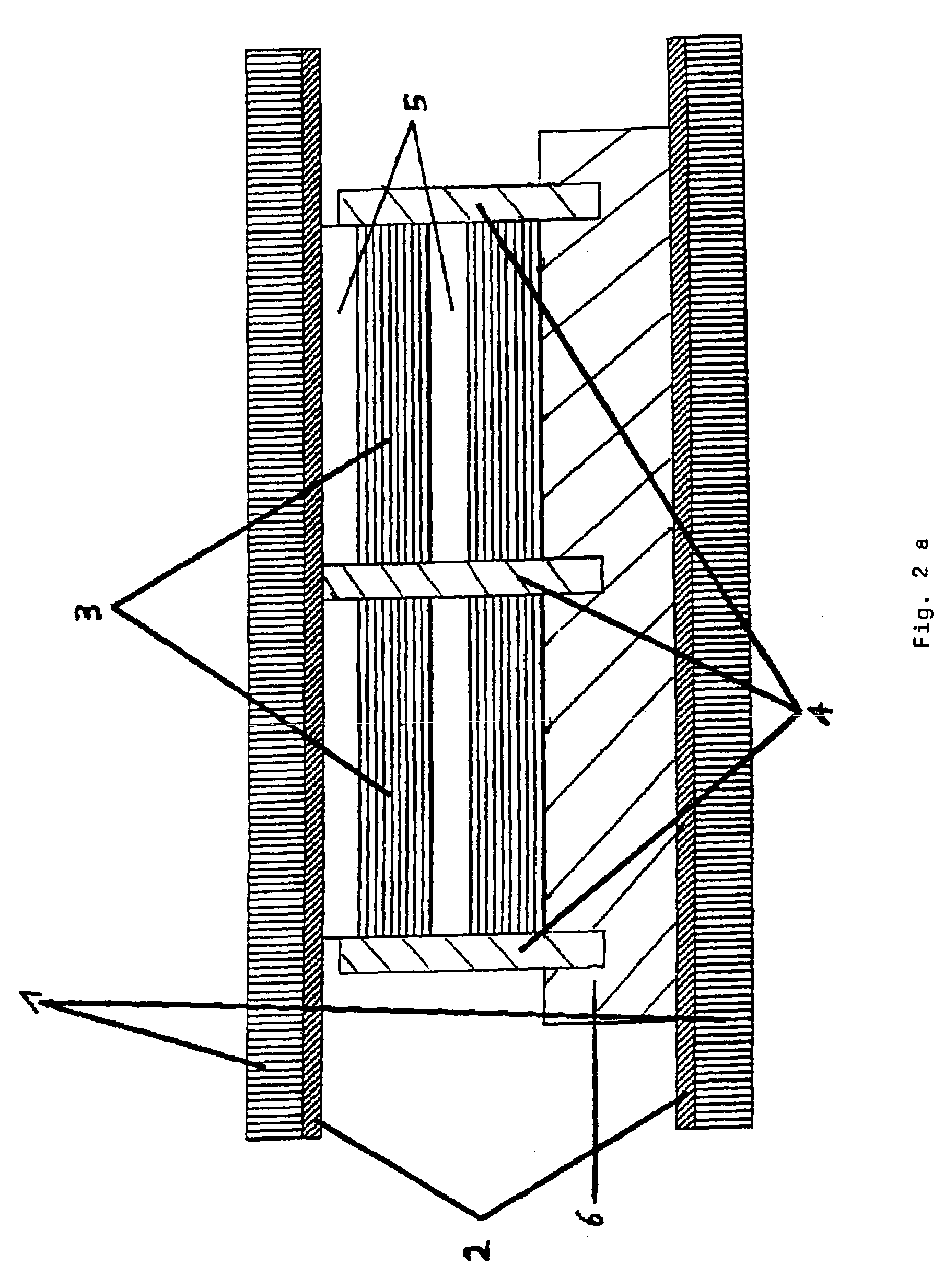
[0147]FIG. 2a illustrates a cross-section of a soldering / brazing structure with microstructure components 3. The microcomponents 3 are registered via registration pins 4 mounted in the bottom plate 6. Pressure is applied via pressure tools 1, whereby the pressure cushions 2 compensate heights between the individual microcomponents 3 and thus enable uniform pressure distribution. FIG. 2b is a top-view of the soldering / brazing structure. It can be seen that the registration pins 4 are mounted on the bottom plate 6. The microcomponents are labeled with the reference number 3.

[0148]FIG. 3 is a cross-sectional side elevation of a template 7 for registering microstructure components 3. The microstructure components 3 are separated from one another in the template 7 by intermediate plates 5. Pressure is applied via pressure tools 1, whereby the pressure cushions 2 compensate heights between the individual microcomponents 3...


PUM

PropertyMeasurementUnit
temperatureaaaaaaaaaa
temperaturesaaaaaaaaaa
melting pointaaaaaaaaaa

Abstract

A method for joining microstructured component layers and a method for manufacturing microstructure component layers and the microstructure component layer is provided. At least one multifunctional barrier coating is applied to the joining surfaces of a base material layer for the microstructured component layers. The layers are made of aluminum/aluminum alloys and/or copper/copper alloys, and/or noble steels. At least one solder/brazing coating is applied to each barrier coating. The coated base material layers comprising the component layers are stacked. The stacked component layers are joined by solder/brazing using heat. The melting temperature of the solder/brazing coating is higher after the heat joining than before same.

Description

BACKGROUND OF THE INVENTION[0001]The invention relates to a method for joining microstructured component layers that are suitable for manufacturing microstructure components and that comprise metals, in particular aluminum and / or aluminum alloys, copper / copper alloys, and / or high-grade steels and furthermore relates to a microstructure component encompassing a stack of microstructured component layers that are joined to one another and that comprise metals and / or metal alloys, in particular aluminum and / or aluminum alloys, copper and / or copper alloys, and / or high-grade steels.[0002]Microstructure components, that is, micro-(μ)-reactors, μ-mixers, and μ-heat exchangers are already employed in chemical process technology and in research and development projects. The first industrial processes have already been realized. For instance, the Clariant Company, Switzerland, jointly with the CPC Company, Germany, installed a pilot system for manufacturing two commercial azo pigments and test...

Claims


Application Information

Patent Timeline
Patent Type & Authority Patents(United States)
IPC IPC(8): B23K31/02B23K1/00B23K1/20B81C99/00B23K35/00B23K35/26B23K35/28B23K35/30B32B15/01B81C1/00C25D7/00
CPCB23K1/0012B23K1/20B23K35/001B23K35/002B23K35/28B23K35/282B23K35/3013B23K35/302B23K35/3066B23K35/3006F28F2260/02B23K2203/04B23K2203/10B23K2203/12B23K35/286B23K35/3033B23K35/3053B23K35/36B23K35/0222B23K35/0233B23K35/0238B23K2103/04B23K2103/10B23K2103/12B81C1/00
Inventor MEYER, HEINRICHCRAMER, KONRADKURTZ, OLAFHERBER, RALPHFRIZ, WOLFGANGSCHWIEKENDICK, CARSTENRINGTUNATUS, OLIVERMADRY, CHRISTIAN
Owner ATOTECH DEUT GMBH
Why Eureka
Try Eureka