Thin film transistor having an etching protection film and manufacturing method thereof

a technology of protection film and thin film transistor, which is applied in the manufacturing of semiconductor/solid-state devices, semiconductor devices, electrical devices, etc., can solve the problems of poor machining accuracy

Inactive Publication Date: 2008-06-10
CASIO COMPUTER CO LTD
View PDF14 Cites 4016 Cited by
  • Summary
  • Abstract
  • Description
  • Claims
  • Application Information

AI Technical Summary

Benefits of technology

[0008]In view of the aforementioned problem, an object of the present invention is to provide a thin film transistor and its manufacturing method that can improve machining accuracy.

Problems solved by technology

However, in the aforementioned manufacturing method, there is a problem in which the zinc oxide easily dissolves in both acid and alkali and its etching resistance is extremely low, thereby causing relatively large side etching in the ZnO semiconductor thin film and the ohmic contact layer formed on the device area in post-process to worsen machining accuracy.

Method used


Image

  • Thin film transistor having an etching protection film and manufacturing method thereof
  • Thin film transistor having an etching protection film and manufacturing method thereof
  • Thin film transistor having an etching protection film and manufacturing method thereof

Examples


first embodiment

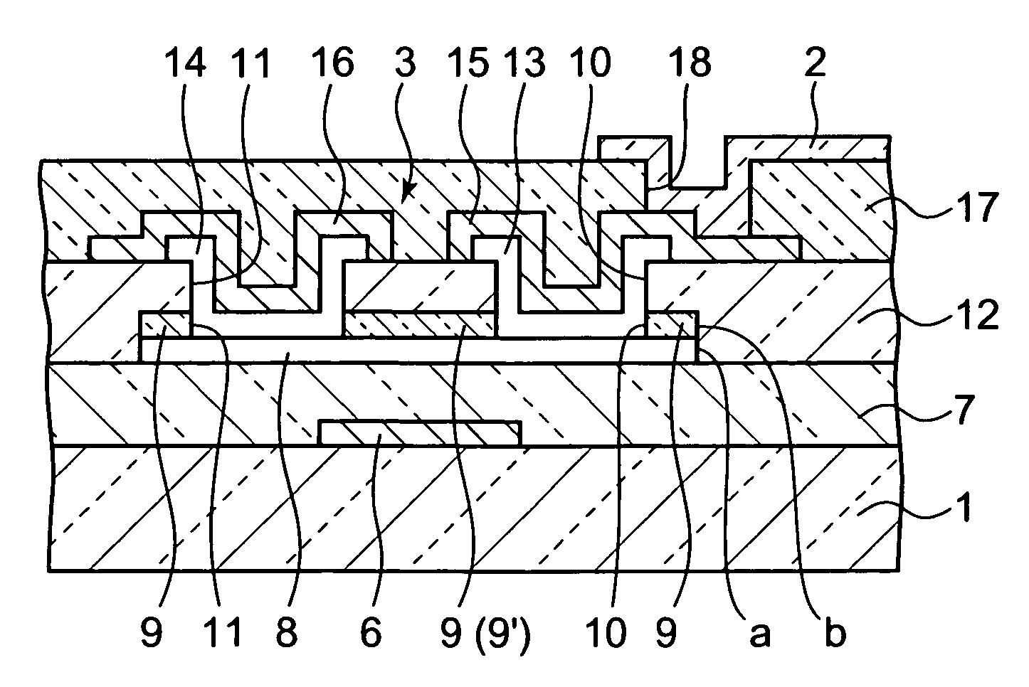
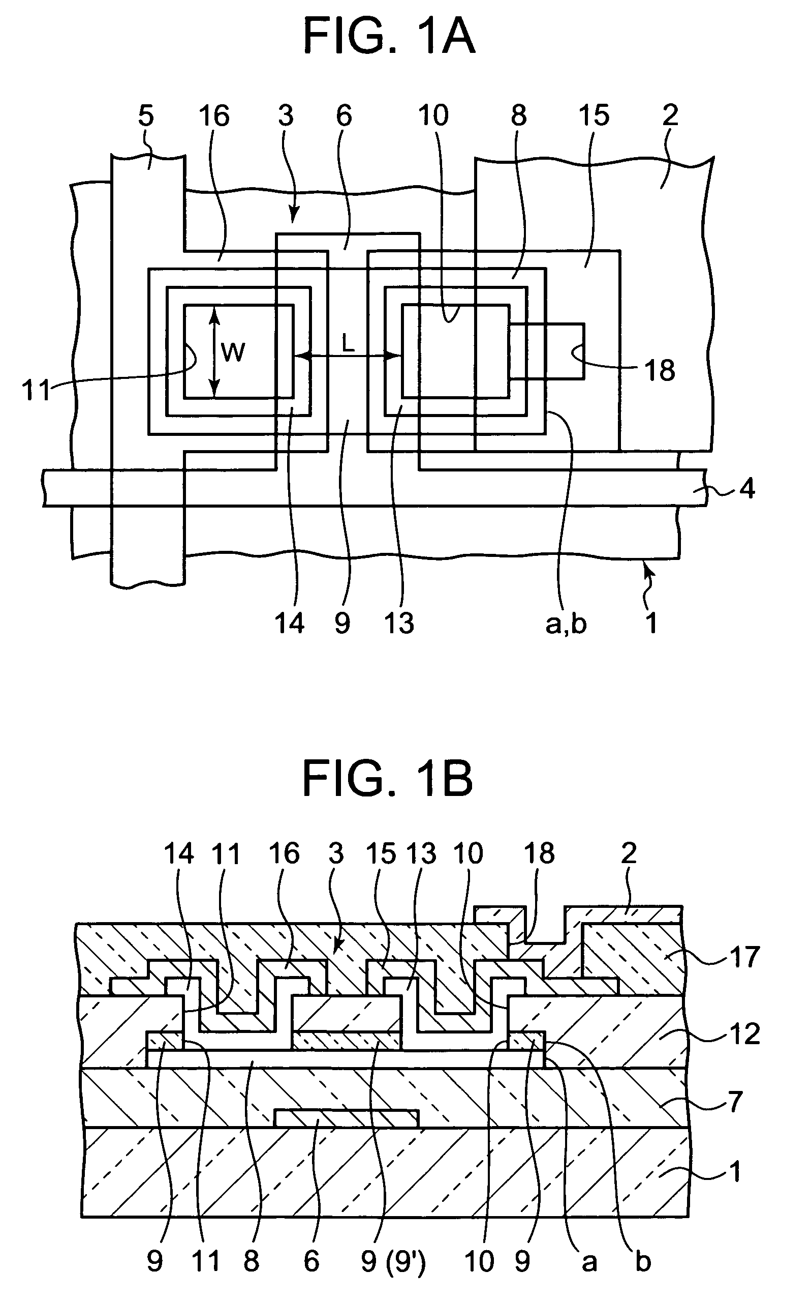
[0037]FIG. 1A is a transparent plan view illustrating a principal part of a liquid crystal display device having a thin film transistor according to a first embodiment of the present invention, and FIG. 1B is a cross sectional view cut along a substantially central line in a channel width direction of the thin film transistor illustrated in FIG. 1A. Additionally, in each of FIGS. 2 to 24 explained below, each of 2B to 24B shows a cross sectional view cut along a substantially central line in a channel width direction of the thin film transistor illustrated in each of FIGS. 2A to 24A. The liquid crystal display device includes a glass substrate 1. On the glass substrate 1, there are formed multiple pixel electrodes 2 arranged in matrix, thin film transistors 3 connected to the pixel electrodes 2, respectively, scanning lines 4 arranged in rows to supply a scanning signal to each thin film transistor 3, and data lines 5 arranged in columns to supply a data signal to each thin film tra...

second embodiment

[0068]FIG. 12A is a transparent plan view illustrating a principal part of a liquid crystal display device having a thin film transistor according to a second embodiment of the present invention and FIG. 12B is a cross sectional view cut along a substantially central line in a channel width direction of the thin film transistor illustrated in FIG. 12A. The liquid crystal display device of the present embodiment is different from that illustrated in FIGS. 1A and 1B in the point that no ohmic contact layers 13 and 14 are provided and the source electrode 15 and the drain electrode 16 are directly connected to the semiconductor thin film 8 through the contact holes 10 and 11.

[0069]Thus, in the case of the semiconductor thin film 8 being made of intrinsic zinc oxide, it was recognized that the thin film transistor 3 was normally operated even if the source electrode 15 and the drain electrode 16, which were formed of aluminum, ITO, etc., were directly connected to the semiconductor thin...

third embodiment

[0073]FIG. 13A is a transparent plan view illustrating a principal part of a liquid crystal display device having a thin film transistor according to a third embodiment of the present invention, and FIG. 13B is a cross sectional view cut along a substantially central line in a channel width direction of the thin film transistor illustrated in FIG. 13A. The liquid crystal display device of the present embodiment is different from that illustrated in FIGS. 1A and 1B in the point that no upper insulating film 12 is provided. Accordingly, the process for film-forming the upper insulating film 12 can be omitted.

[0074]However, in this case, after the contact hole forming process as illustrated in FIGS. 6A and 6B, when the resist pattern (not shown), which is used in forming the contact holes 10 and 11 on the protection film 9, is stripped using a resist stripper, the peripheral end surface of the semiconductor thin film 8 is exposed to the resist stripper to cause side etching slightly on...


PUM


Abstract

A thin film transistor of the present invention includes a semiconductor thin film (8); a gate insulating film (7) formed on one surface of the semiconductor thin film (8); a gate electrode (6) formed to be opposite to the semiconductor thin film (8) through the gate insulating film (7); a source electrode (15) and a drain electrode (16) electrically connected to the semiconductor thin film (8); a source region; a drain region; and a channel region. The thin film transistor further includes an insulating film (9) formed on a peripheral portion corresponding to at least the source region and the drain region of the semiconductor thin film (8), and having a contact hole (10, 11) through which at least a part of each of the source region and the drain region is exposed wherein the source electrode (15) and the drain electrode (16) are connected to the semiconductor thin film (8) through the contact hole (10, 11).

Description

[0001]This application is based on Japanese Patent Application No. 2004-255307 filed on Sep. 2, 2004 and Japanese Patent Application No. 2004-378476 filed on Dec. 28, 2004 and including specification, claims, drawings and summary. The disclosures of the above Japanese Patent Applications are incorporated herein by reference in their entireties.BACKGROUND OF THE INVENTION[0002]1. Field of the Invention[0003]The present invention relates to a thin film transistor having an etching protection film and manufacturing method thereof.[0004]2. Description of the Related Art[0005]Unexamined Japanese Patent Application KOKAI Publication H 5-67786 discloses a structure as a thin film transistor used as a switching element of an active matrix liquid crystal display device. The thin film transistor includes a gate electrode formed on an upper surface of an insulating substrate, a gate insulating film formed on the upper surface of the insulating film including the gate electrode, an intrinsic am...

Claims


Application Information

Patent Timeline
Patent Type & Authority Patents(United States)
IPC IPC(8): H01L29/04H01L27/14H01L29/15H01L31/036
CPCH01L29/41733H01L29/45H01L29/78618H01L29/66969H01L29/7869H01L29/458H01L29/66742H01L29/78696
Inventor ISHII, HIROMITSUHOKARI, HITOSHIYOSHIDA, MOTOHIKOYAMAGUCHI, IKUHIRO
Owner CASIO COMPUTER CO LTD
Why Eureka
Try Eureka