

Exposure apparatus and method
a technology of exposure apparatus and exposure, applied in the field of exposure, can solve the problems of deteriorating imaging performance, affecting the quality of image processing, and not being able to meet the demand for finer processing, so as to maintain imaging performance and yield
- Summary
- Abstract
- Description
- Claims
- Application Information
AI Technical Summary
Benefits of technology
Problems solved by technology
Method used
Image

Examples
Embodiment Construction
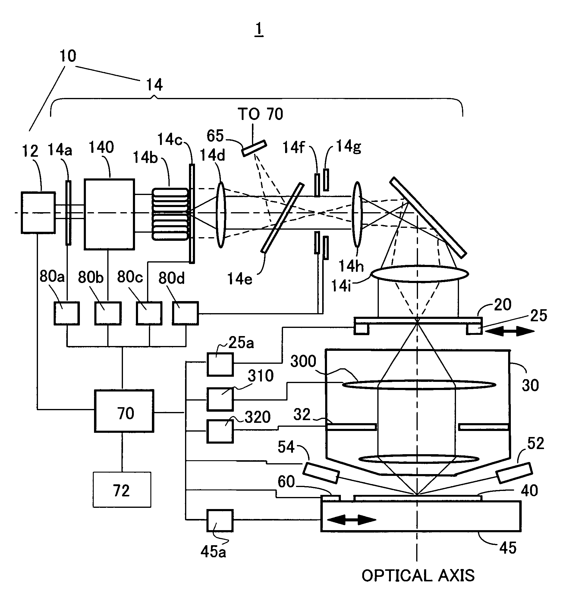
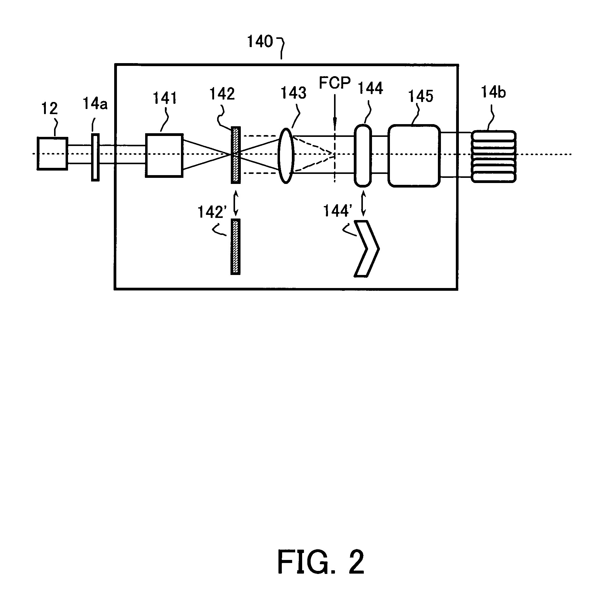
[0027]Referring now to the accompanying drawings, a description will be given of the exposure apparatus 1 according to one aspect of the present invention. In each figure, those elements, which are the corresponding elements, are designated by the same reference numerals, and a duplicate description thereof will be omitted. FIG. 1 is a schematic block diagram of the exposure apparatus 1.
[0028]The exposure apparatus 1 is a projection exposure apparatus that exposes a circuit pattern of a reticle 20 onto an object 40, e.g., in a step-and-repeat or a step-and-scan manner. Such an exposure apparatus is suitable for a sub-micron or quarter-micron lithography process, and this embodiment exemplarily describes a step-and-scan exposure apparatus (which is also called “a scanner”). The “step-and-scan manner”, as used herein, is an exposure method that exposes a mask pattern onto a wafer by continuously scanning the wafer relative to the mask, and by moving, after a shot of exposure, the wafe...
PUM
| Property | Measurement | Unit |
|---|---|---|
| wavelength | aaaaa | aaaaa |
| wavelength | aaaaa | aaaaa |
| wavelength | aaaaa | aaaaa |
Abstract
Description
Claims
Application Information