Pixel detector and method of manufacture and assembly thereof

a technology of pixel detector and detector body, which is applied in the direction of x/gamma/cosmic radiation measurement, instruments, radioation controlled devices, etc., can solve the problems of low yield, difficult to increase the resolution of the sensor, and conventional silicon diodes are not suitable for such applications, so as to avoid the effect of dead space in the central region

Active Publication Date: 2008-06-17
RAPISCAN LAB INC
View PDF14 Cites 4 Cited by
  • Summary
  • Abstract
  • Description
  • Claims
  • Application Information

AI Technical Summary

Benefits of technology

[0023]It is thus an object of the invention to provide a pixel sensor array particularly suitable for use with X-ray imaging that obviates the need to provide conductive vias through the silicon wafer, but nevertheless avoids dead space in the central regions of the detector.

Problems solved by technology

Conventional silicon diodes are not suitable for such applications because they are transparent to the high-energy photons and therefore other materials such as cadmium telluride or mercuric iodide are used instead.
Since these materials are not based on silicon, the diode cannot be integrated together with the associated electronics as a single monolithic structure and this requires, in practice, that the sensor elements and the associated electronics be manufactured on separate wafers, which are then interconnected using bump bonding.
On the one hand, the bump bonding technique used in conventional pixel sensors militates against the closer packing density of the pixels so that it becomes difficult to increase the resolution of the sensor by packing more pixels into a pixel array, since the need to bump-bond each sensor to the corresponding electronics in a different array is a costly process and is subject to low yields.
Furthermore, the provision of control-pads along an edge of each module and the need to wire bond these pads to external circuitry means that adjacent sensor arrays cannot be packed edge-to-edge without introducing a “dead” zone where there are, in fact, no pixels at all owing to the interposing I / O and control-pads.
Moreover, the connection of the I / O control-pads to the external circuitry by wire bonding is also a costly and cumbersome process and further reduces the effective overall packing density.
The small size of hitherto-proposed sensor arrays such as shown in FIG. 2 having contact pads at an edge on the one hand militates against their use as standalone X-ray or γ-ray detectors and, on the other hand, renders it inevitable that when juxtaposed edge to edge there will be created dead spaces in the central regions of the detector which are insensitive to incoming photons.
This solution is effective but the need to provide the conductive vias complicates the manufacturing process.
Such an approach is prone to inaccuracy since the light generated by the scintillator is apt to disperse and strike adjacent pixels of the photodetector array thereby resulting in poor spatial resolution.
Moreover, scintillator detectors have poorer Detection Quantum Efficiency leading to higher patient dosage.

Method used


Image

  • Pixel detector and method of manufacture and assembly thereof
  • Pixel detector and method of manufacture and assembly thereof
  • Pixel detector and method of manufacture and assembly thereof

Examples


Embodiment Construction

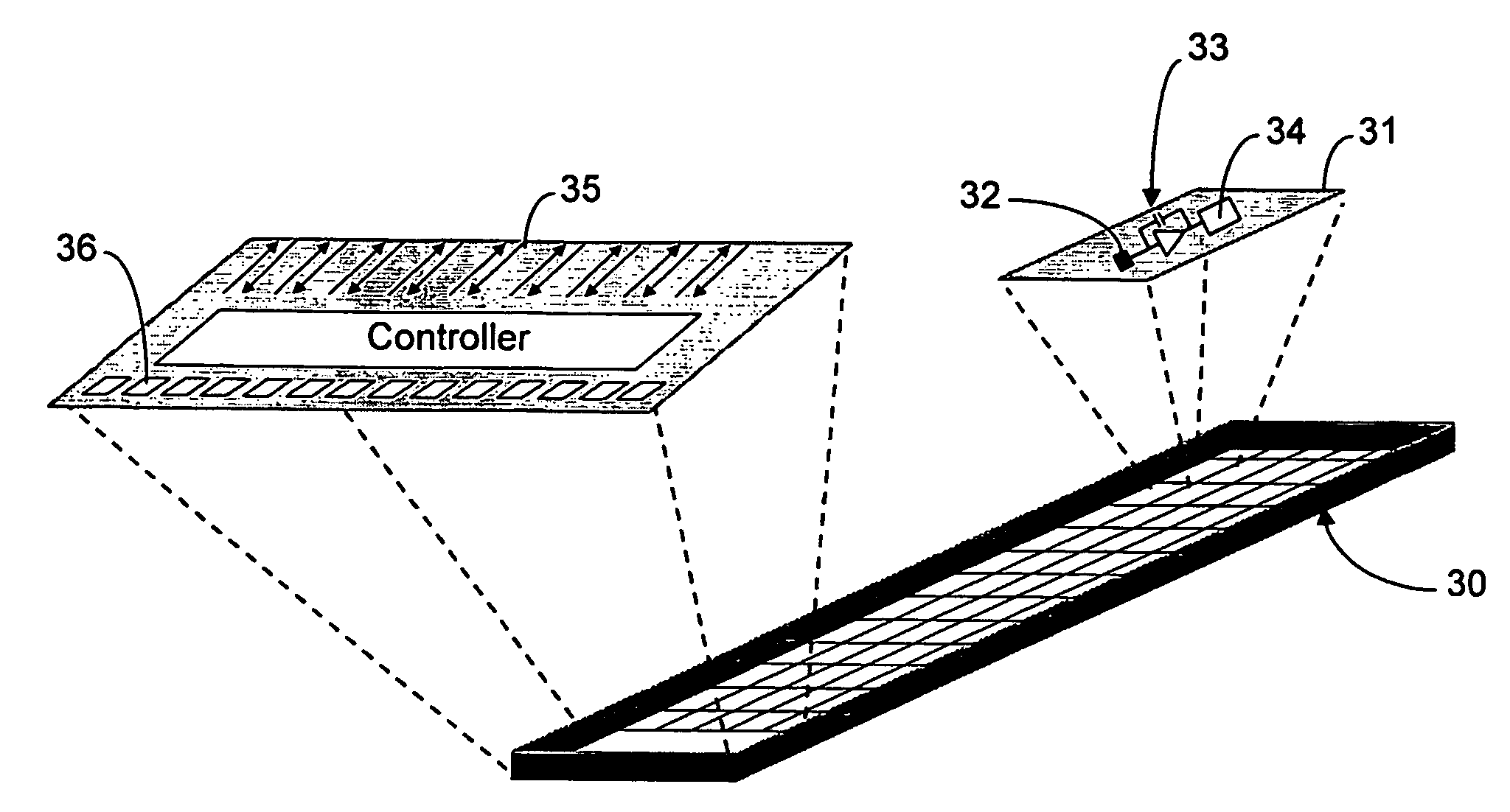
[0040]The present invention is based on the fabrication of different architectures on a single CMOS wafer using “stitching”. To this end, it will aid in appreciating the inventive concept of the present invention if a brief introduction to stitching is presented even though the technique is not novel per se. On the other hand, a sensor array manufactured according to the invention is visibly distinguished from hitherto known sensor arrays on account of the stitching and it is therefore important that the distinction be appreciated.

[0041]In the fabrication of CMOS circuits, thin wafers are sliced from bulk pure silicon. Each thin wafer may have a diameter of approximately 30 cm (12″) and from this single wafer multiple integrated circuits (ICs) are produced using known lithographic techniques. Commonly a large number of identical ICs are fabricated from a single wafer and, to this end, artwork masks corresponding to the desired IC circuitry are imaged at spaced apart intervals to for...


PUM


Abstract

A detector assembly (50) is formed by integrating the electronic processing circuits on a CMOS wafer by stitching a plurality of reticles of at least two different types so as to form an integrated circuit having an array of electronic processing circuits each having a respective sensor input disposed toward a first surface of the wafer and accessible from the first surface via a contact formed near an edge of the integrated circuit. Sensor elements (56) are disposed on the first surface of the respective integrated circuits in the detector whereby an exposed surface of the sensor elements forms a common first electrode towards which incident photons are directed, and an opposite unexposed surface thereof forms multiple second electrodes of opposite polarity to the first electrode each in registration with a corresponding sensor input.

Description

FIELD OF THE INVENTION[0001]This invention relates to pixel sensors for use in X-ray and γ-cameras.BACKGROUND OF THE INVENTION[0002]Pixel sensors are known to comprise an array of sensor elements such as diodes, and a complementary array of electronics, typically in the form of an ASIC and comprising a charge amplifier and processing electronics for each sensor element. In CCDs such as are used in miniature television cameras and the like, the sensor elements are formed of silicon diodes which are responsive to visible light for producing a current which is amplified by the charge amplifier and subsequently processed.[0003]Pixel sensors for X-ray and nuclear medical imaging are known that respond to high-energy photons such as X-rays or γ-rays and produce charge in a similar manner. Conventional silicon diodes are not suitable for such applications because they are transparent to the high-energy photons and therefore other materials such as cadmium telluride or mercuric iodide are u...

Claims


Application Information

Patent Timeline
Patent Type & Authority Patents(United States)
IPC IPC(8): H01L27/00H01L27/06H01L27/148H01L31/02
CPCH01L27/14634H01L27/1469H01L27/14692H01L31/02002
Inventor NYGARD, EINAR
Owner RAPISCAN LAB INC
Why Eureka
Try Eureka