
Method of compensating for etch effects in photolithographic processing

a technology of photolithographic processing and mask/reticle data, applied in the field of photolithographic processing, can solve the problems of processing distortion that affects a wafer, etch effect, more complex and severe distortion,

Active Publication Date: 2008-06-24
SIEMENS PROD LIFECYCLE MANAGEMENT SOFTWARE INC
View PDF19 Cites 19 Cited by
  • Summary
  • Abstract
  • Description
  • Claims
  • Application Information

AI Technical Summary

Benefits of technology

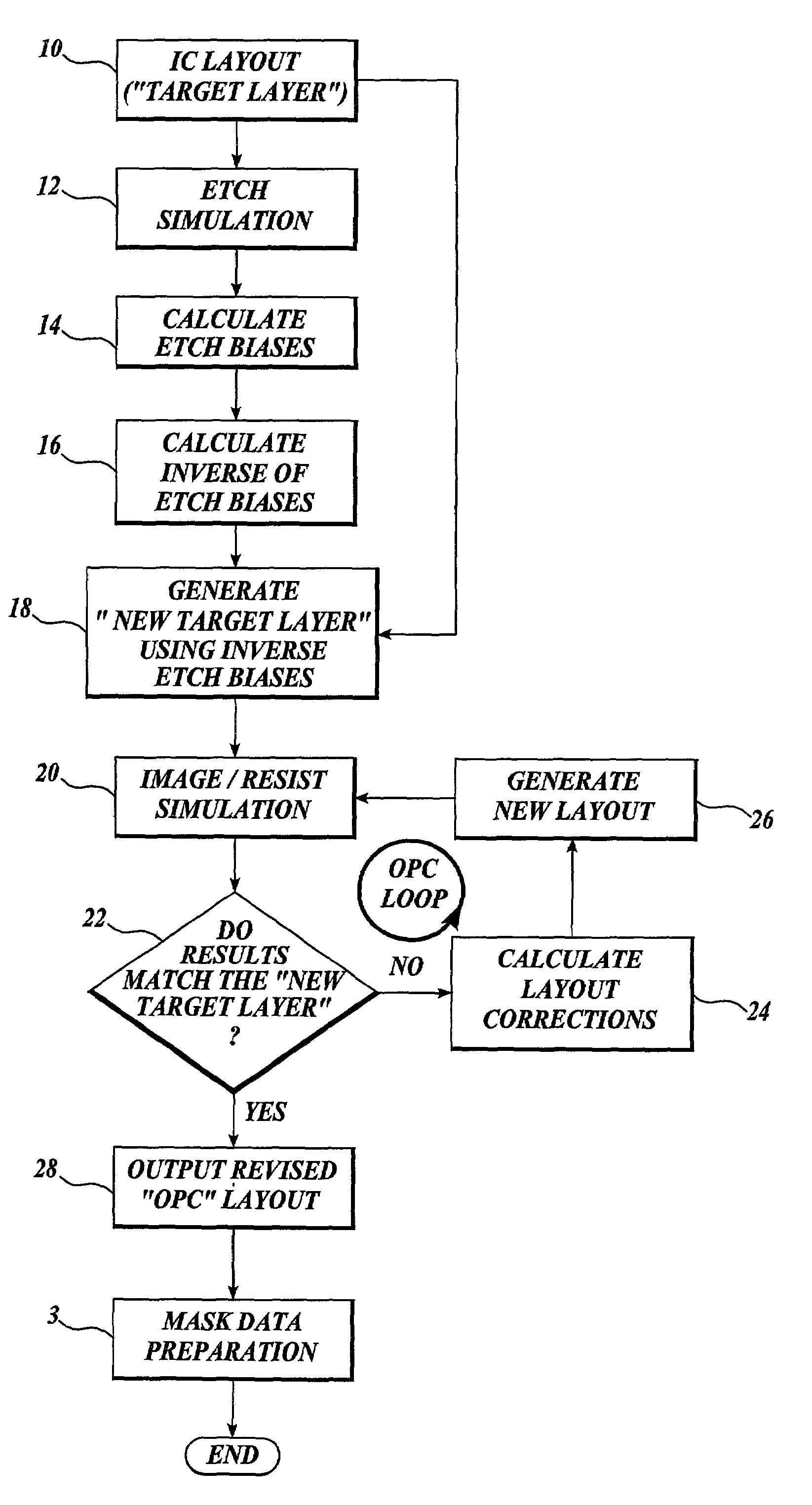
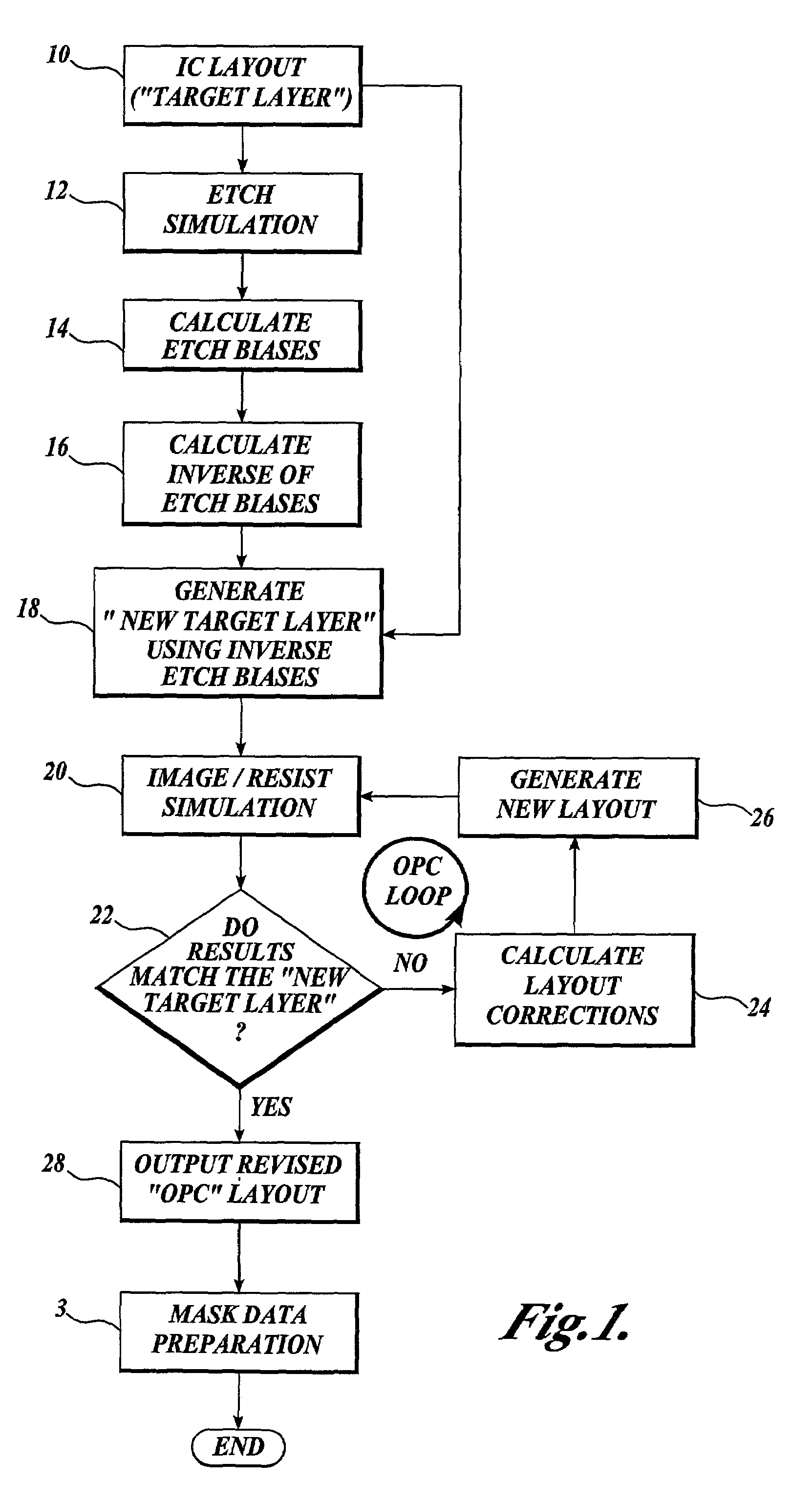
[0008]A method of compensating layout data to be used in creating a mask or reticle for photolithographic process distortions and, in particular, etch process distortions. In one embodiment, the method includes the acts of reading a first set of mask / reticle data that defines a target layer to be created when a wafer is exposed through the mask / reticle. A simulation of the etch effects occurring on a wafer created using the first set of data is performed to determine etch biases or an estimate of the size of the objects that will be created on the wafer versus the size specified by the target layer. It should be noted that the simulation can be a traditional physics-based process simulation, but can also comprise a simpler model where predetermined values are accessed or produced by a set of rules or by accessing a look-up table. The inverse of the estimated etch biases are used to create a second set of mask / reticle data that defines a new target layer that is compensated for the etch distortion. A simulation of other optical process distortions is performed using the new target layer as an input. The mask / reticle data is then compensated for optical process distortions and the compensated set of data is then exported to a mask / reticle writer to manufacture a corresponding mask / reticle.

Problems solved by technology

However, as patterns became more intricate and distortions more severe, model-based OPC techniques were developed.
Another processing distortion that affects a wafer is the etch effect, whereby the patterns that are etched on the surface of a wafer differ from a desired pattern.
However, in practice the results are often inaccurate.
This is because the physical phenomena of etching, such as density-based microloading and certain etch shadowing effects are non-linear and not well described by the linear mathematics of convolution.
However, etch simulators tend to be computationally intensive and the addition of an etch simulator within each pass of an OPC loop can make the OPC correction process impractical to implement.

Method used


Image

  • Method of compensating for etch effects in photolithographic processing
  • Method of compensating for etch effects in photolithographic processing
  • Method of compensating for etch effects in photolithographic processing

Examples


Embodiment Construction

[0013]As indicated above, the present invention is a method for compensating mask / reticle data for process distortions that occur on a wafer during photolithographic processing and particularly during etch processing.

[0014]In accordance with one embodiment of the present invention, and as shown in FIG. 1, a computer system of the type including one or more processors (not shown), executes a sequence of program steps stored on a computer-readable media to cause the computer to read an IC layout or data file at a step 10 that defines a number of features to be placed on a mask / reticle. These features will define corresponding objects on a wafer when the wafer is exposed using the mask / reticle. The mask / reticle data can be referred to as a “target layer” when it defines the desired size / shape of the objects to be created on the wafer after processing. At a step 12, an etch simulation is performed that determines the likely effects of how the size or shape of the objects created on the ...


PUM

PropertyMeasurementUnit
distanceaaaaaaaaaa
diametersaaaaaaaaaa
diameteraaaaaaaaaa

Abstract

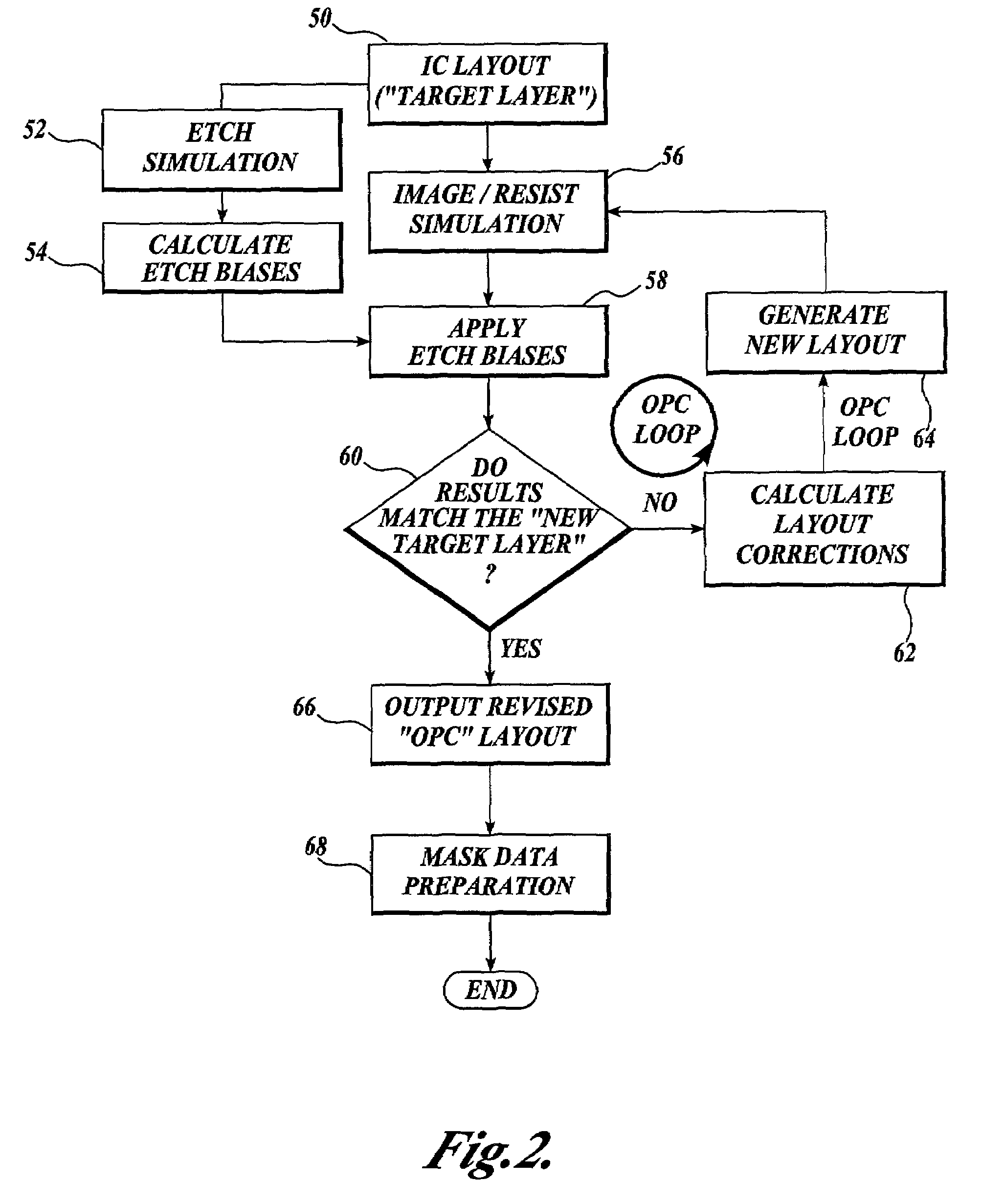
A computer system reads data corresponding to an IC layout target layer and performs an etch simulation on the target layer. Etch biases are calculated and the inverse of the etch biases are used to produce a new target layer. The new target layer is provided as an input to an optical process correction (OPC) loop that corrects the data for image / resist distortions until a simulation indicates that a pattern of objects created on a wafer matches the new target layer. In another embodiment of the invention, original IC layout data is provided to both the OPC loop and an etch simulation. Etch biases calculated by the etch simulation are used in the OPC loop in order to produce mask / reticle data that will be compensated for both optical and resist distortions as well as for etch distortions.

Description

RELATED APPLICATIONS[0001]The present application is related to U.S. Provisional Application No. 60 / 275,673 filed Mar. 13, 2001, and claims the benefit of the filing date under 35 U.S.C. § 119.FIELD OF THE INVENTION[0002]The present invention relates to photolithographic processing, and in particular, to methods of compensating mask / reticle data for etch process distortions.BACKGROUND OF THE INVENTION[0003]As integrated circuit (IC) features become smaller, process distortions have a growing impact on pattern fidelity in manufacturing and, in turn, on device performance. Examples of process distortions include pattern-dependent line-width biasing, corner rounding, and line end shortening, all of which create patterns on a wafer that are different than patterns defined on a corresponding mask or reticle.[0004]In recent years, optical process correction (OPC) techniques have been developed that compensate for distortions that occur in printing. Originally, OPC modifications could be a...

Claims


Application Information

Patent Timeline
Patent Type & Authority Patents(United States)
IPC IPC(8): G06F17/50G06F13/12G03F1/00G03F1/36
CPCG03F1/144G03F1/36G03F1/80
Inventor GRANIK, YURISCHELLENBERG, FRANKLIN M.
Owner SIEMENS PROD LIFECYCLE MANAGEMENT SOFTWARE INC
Learn More