Wiring board and semiconductor package using the same

a technology of wiring board and semiconductor package, applied in the direction of semiconductor/solid-state device details, printed circuit aspects, printed element electric connection formation, etc., can solve the problems of loop inductance becoming high, deformation occurring, and difficult control of impedance, so as to achieve high-speed transmission and reliable

Inactive Publication Date: 2008-07-08
NEC CORP +1
View PDF12 Cites 59 Cited by
  • Summary
  • Abstract
  • Description
  • Claims
  • Application Information

AI Technical Summary

Benefits of technology

[0016]An object of the present invention is to provide a reliable wiring board, which is capable of including various devices such as a semiconductor device at high densities and which makes it possible to easily implement a high-speed transmission and a high-density fine wiring, and a semiconductor package using the wiring board.
[0027]In contrast, by using the insulating film having the physical properties achieved by the invention, strain stress can be reduced in the direction of thickness. Because of this, when heat load is repeatedly applied through the operation of the semiconductor device in the state that the via holes are formed immediately under the electrode pads on which the semiconductor is mounted, and then the solder balls used for board mounting are provided immediately under the via holes, it is possible to prevent the open failure at the via hole junctions, so that a more reliable semiconductor package can be obtained.
[0038]Further, in these wiring boards, a concave portion is formed on the under surface of the base insulating film, and then in order to improve positional accuracy of the mounting of the semiconductor device having pads with a narrow pitch through the use of solder, it is preferable that the lower wiring be embedded in the concave portion, and the under surface of the lower wiring be located higher than the under surface of the base insulating layer by 0.5 to 10 μm.
[0039]Still further, when the under surface of the base insulating film and the under surface of the lower wiring are made coplanar, a margin for positional deviation can be obtained in the step of mounting the semiconductor device having pads with a narrow pitch through the use of gold bumps or the like, so that it is preferable in terms of improvement of connection reliability.
[0040]Also, the wiring board may have a protective film, which is formed under the base insulating film, covers a part of the lower wiring, and exposes the remainder. Furthermore, the wiring board may have a solder resist layer, which covers a part of the upper wiring and which exposes the remainder. Therefore, solder can be readily formed on the wiring board by printing or the like, and further when a semiconductor device having pads with a very narrow pitch is mounted, metal bumps, such as solder and gold, formed on the semiconductor device can be connected to the solder provided on the wiring board by fusing, so that it is possible to obtain a semiconductor package which has outstanding reliability of the bump connections.
[0042]The present invention can provide wiring boards which allowed for implementation of a high-speed transmission and high-density fine wiring by using an insulating film having low temperature dependence mechanical properties as a base insulating film, has no crack generation at the base insulating film, solder balls, or the like when heat load is repeatedly applied by the driving of a semiconductor device mounted, and has excellent reliability of via hole connections.

Problems solved by technology

However, the built-up printed board has an insufficient heat resistance due to the use of a glass epoxy printed board as the base core substrate 73, so that there is a problem deformations occur with the base core substrate 73, such as shrinkage, warpage and waviness through heat treatment performed for forming the interlayer insulating film 75.
Even though a wiring having provision for high-speed operation is designed on the built-up layer having the interlayer insulating film 75 and the conductor wiring 76, the control of impedance becomes difficult and loop inductance becomes high due to the presence of the land portions.
Because of this, the operating speed of the entire built-up printed board is reduced, which brings about a problem that it is difficult to make the provision for high-speed operation.
However, in this conventional art, a positional accuracy in the lamination of the prepregs 82 is low, which brings about a problem that it is difficult to reduce the diameter of the land pattern 86.
Therefore, it is difficult to implement high-density wiring, and the effects of improving the controllability of the impedance and of decreasing the loop inductance are insufficient.
Furthermore, there is a problem that the reliability of the through hole connectivity after the lamination is poor.
However, the conventional art has a problem described below.
Because of this, there is a problem that it is impossible to secure reliability required for the wiring board and the semiconductor packages.

Method used


Image

  • Wiring board and semiconductor package using the same
  • Wiring board and semiconductor package using the same
  • Wiring board and semiconductor package using the same

Examples


first embodiment

[0057]In the following, embodiments of the present invention will be described specifically with reference to the accompanying drawings. First, the invention will be described. FIG. 4 is a cross-sectional view showing a wiring board according to the embodiment, and FIG. 5 is a cross-sectional view showing a semiconductor package according to the embodiment.

[0058]As shown in FIG. 4, a wiring board 13 according to the embodiment is provided with a base insulating film 7. The base insulating film 7 is made of a heat-resistant resin having a glass-transition temperature of 150° C. or more and containing reinforcing fiber made of glass or aramid. The base insulating film 7 has a thickness of 20 to 100 μm and has the following physical properties (1) to (6) when the elastic modulus thereof at a temperature of T° C. is given as DT (GPa) and the breaking strength thereof at a temperature of T° C. is given as HT (MPa).[0059](1) A coefficient of thermal expansion in the direction of thickness...

second embodiment

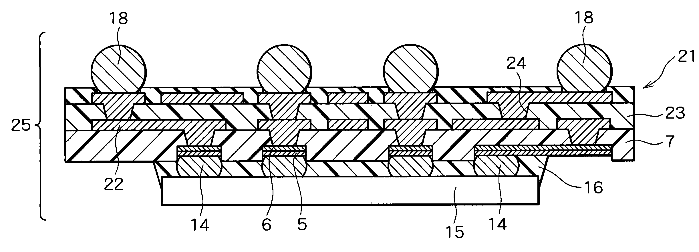
[0093]Next, a second embodiment according to the invention will be described. FIG. 7 is a cross-sectional view showing a wiring board according to the embodiment, and FIG. 8 is a cross-sectional view showing a semiconductor package according to the embodiment.

[0094]As shown in FIG. 7, a wiring board 21 according to the embodiment is provided with the base insulating film 7. The thickness and mechanical properties of the base insulating film 7 are the same as those of the base insulating film 7 of the first embodiment. The concave portions 7a are formed in the under surface of the base insulating film 7, the wiring body 6 is formed in the concave portion 7a, and the etching barrier layer 5 is formed under the wiring body 6. The lower wiring is composed of the etching barrier layer 5 and the wiring body 6, and the lower wiring is embedded in the concave portion 7a. The configuration of the etching barrier layer 5 and the wiring body 6 is the same as that of the first embodiment.

[0095]...

third embodiment

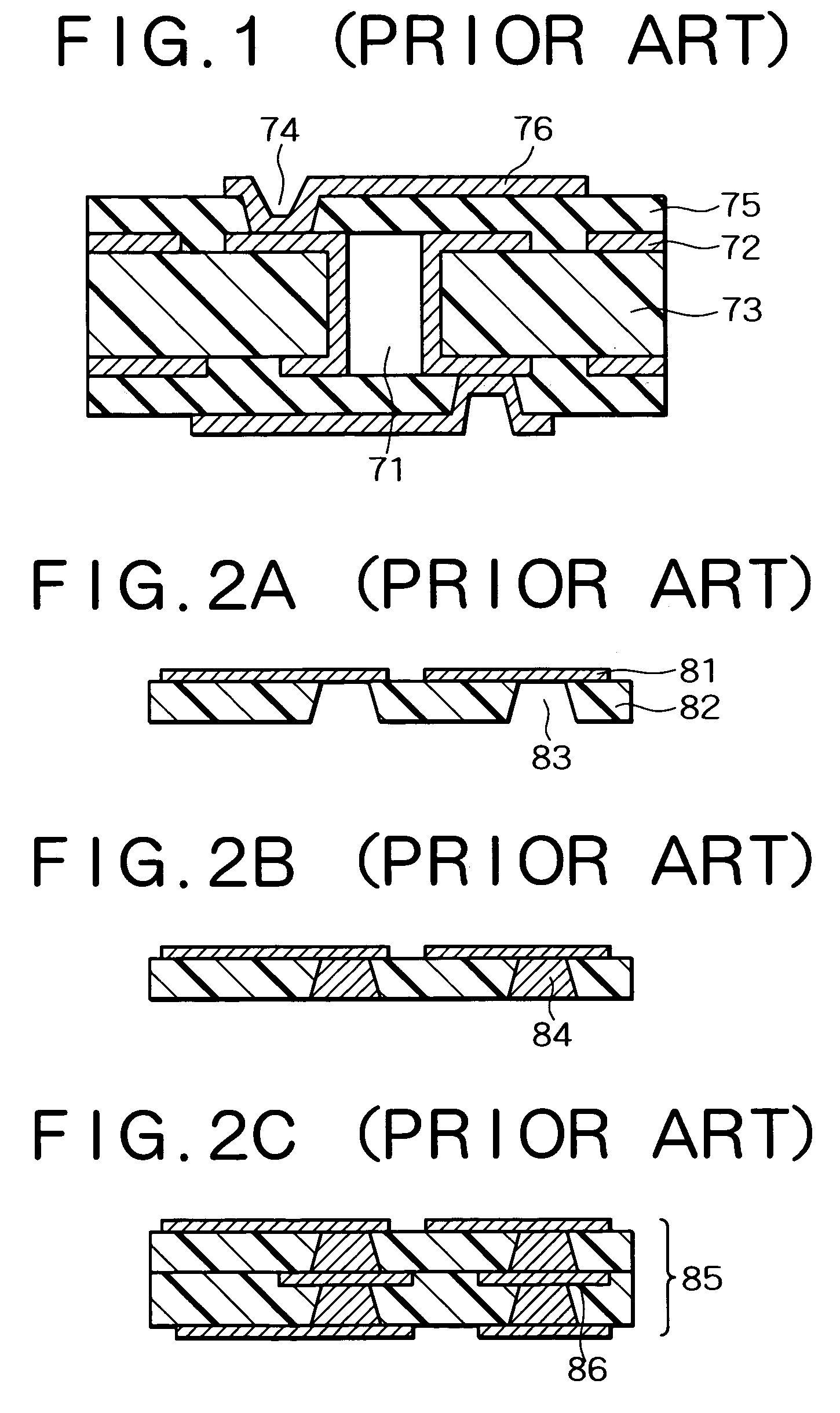
[0118]Next, a method for manufacturing the wiring board will be described. To begin with, as shown in FIG. 9A, the protective film 41 is applied to the entire upper surface of the supporting substrate 1 by, for instance, laminating or pressing to form a film. Then, for instance, the film is heat treated in a manner that the film is held for 10 minutes to 2 hours at a temperature of 100 to 400° C. to harden the protective film 41. The temperature and the time of the heat treatment are suitably adjusted according to the materials of which the protective film 41 is made. The thickness of the protective film 41 is, for instance, 1 to 50 μm.

[0119]Next, a resist (not shown) is formed on the protective film 41 to perform patterning. The lower layer composed of the etching barrier layer 5 and the wiring body 6 is formed in the region where the resist has been removed. Furthermore, the base insulating film 7 is formed so as to cover the lower wiring, the via holes 10 are formed in the base ...


PUM

PropertyMeasurementUnit
thicknessaaaaaaaaaa
glass-transition temperatureaaaaaaaaaa
diameteraaaaaaaaaa

Abstract

A wiring board has a base insulating film. The base insulating film has a thickness of 20 to 100 μm and is made of a heat-resistant resin which has a glass-transition temperature of 150° C. or higher and which contains reinforcing fibers made of glass or aramid. The base insulating film has the following physical properties (1) to (6) when an elastic modulus at a temperature of T° C. is given as DT (GPa) and a breaking strength at a temperature of T° C. is given as HT (MPa).(1) A coefficient of thermal expansion in the direction of thickness thereof is 90 ppm / K or less(2) D23≧5(3) D150≧2.5(4) (D−65 / D150)≦3.0(5) H23≧140(6) (H−65 / H150)≦2.3.

Description

BACKGROUND OF THE INVENTION[0001]1. Field of the Invention[0002]The present invention relates to a wiring board suitably used for semiconductor packages and modules and to a semiconductor package using the wiring board. More particularly the invention relates to a wiring board, which is capable of including various devices, such as semiconductor devices, in high density, and driving these devices at high speed and which has improved reliability, and to a semiconductor package using the wiring board.[0003]2. Description of the Related Art[0004]In recent years, accompanying an increase in the number of terminals, their narrowed pitches, and increased operation speeds in semiconductor devices which result from the trend toward higher performance and greater functions of the devices, there has been growing demand that wiring boards for packaging provided with the semiconductor device attain higher-density finer wiring and higher-speed operation. As an example of conventional wiring boar...

Claims


Application Information

Patent Timeline
Patent Type & Authority Patents(United States)
IPC IPC(8): H05K1/00H01L23/12H01L21/48H01L21/68H01L23/14H01L23/498H01L25/065H05K1/03H05K1/11H05K3/20H05K3/42
CPCH01L21/4857H01L21/6835H01L23/145H01L23/49816H01L23/49822H01L25/0657H05K1/0366H01L2221/68345H01L2224/16225H01L2224/16237H01L2224/32014H01L2224/48091H01L2224/48227H01L2224/73265H01L2224/83102H01L2224/92125H01L2225/0651H01L2225/06517H01L2225/06586H01L2924/01046H01L2924/01078H01L2924/01079H01L2924/09701H01L2924/15311H01L2924/1532H01L2924/30107H01L2924/3011H05K3/205H05K3/423H05K2201/0376H05K2201/068H05K2203/0733H01L24/48H01L2924/01019H01L2924/01087H01L2224/32145H01L2224/32225H01L2224/73204H01L2924/10253H01L2924/00014H01L2924/00H01L2924/00012H01L2924/12042H01L24/73H01L2924/14H01L2924/181H01L2224/45099H01L2224/45015H01L2924/207
Inventor SHIMOTO, TADANORIKIKUCHI, KATSUMIMURAI, HIDEYABABA, KAZUHIROHONDA, HIROKAZUKATA, KEIICHIRO
Owner NEC CORP
Why Eureka
Try Eureka