Impurity measuring method for Ge substrates

a technology of impurity measurement and ge substrate, which is applied in the field of impurity measurement on ge substrate, can solve the problems of not working in the case of ge wafer, lack of metallic contamination analysis of ge wafer, and severe limitations in the use of methodology to achieve large wafer sizes

Active Publication Date: 2008-07-15
N V UMICORE
View PDF6 Cites 6 Cited by
  • Summary
  • Abstract
  • Description
  • Claims
  • Application Information

AI Technical Summary

Problems solved by technology

Whereas several studies focused on the optimization of cleaning recipes, there is still a lack in the metallic contamination analysis for Ge wafers.
This technique, however, does not work in case of Ge wafers, because an aqueous mixture is not phobic to Ge and droplet loss occurs during scanning.
However, this methodology suffers from severe limitations with respect to automation and scalability to large wafer sizes.
This treatment resulted in rather hydrophilic surfaces.

Method used


Image

  • Impurity measuring method for Ge substrates
  • Impurity measuring method for Ge substrates
  • Impurity measuring method for Ge substrates

Examples


example

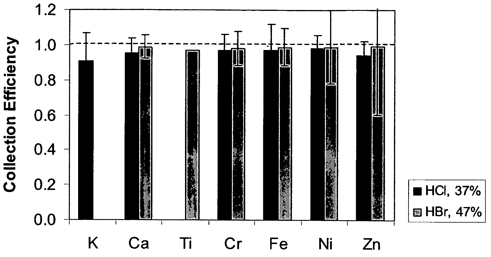
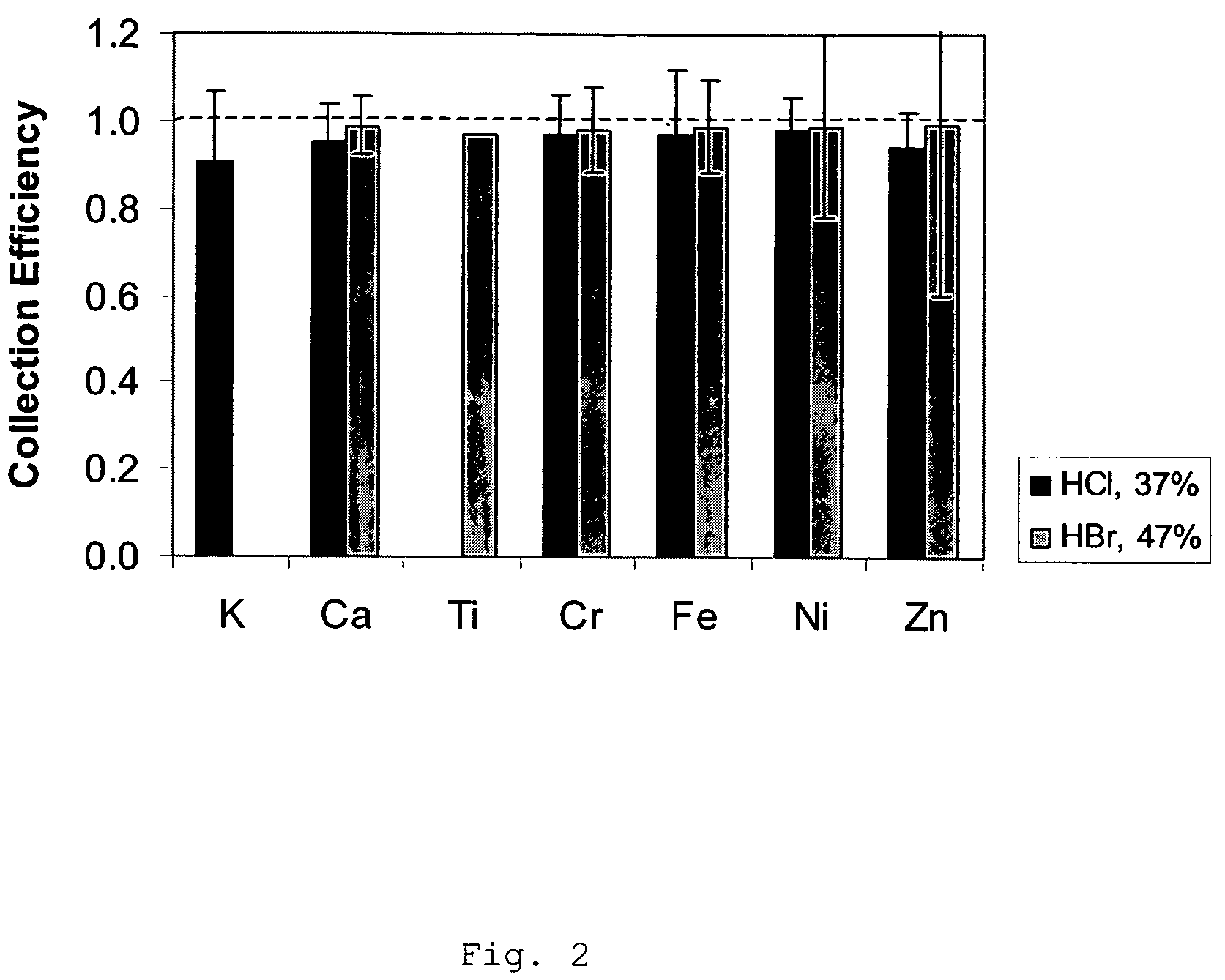
[0085]In this example, a 100 mm Ge wafers (Umicore) and 200 mm Si wafers, both with a crystal orientation, were used.

[0086]Ge droplet residues standards were prepared by the micro-droplet deposition method.

[0087]Standard multi-element solutions with a constant concentration of traces (K, Sc, Cr, Fe, Ni, Zn, all at 2.5×10¹² atoms / 50 μL) and a variable Ge concentration were prepared by dilution of ICP-MS calibration standards (1000 μg / mL, nitrate salts, Merck).

[0088]Droplets of 50 μL volume were pipetted on hydrophobic Si wafers (contact angle 65 deg) and dried at 50° C. and 100 mbar in a Wafer Surface Preparation System (GeMeTec).

[0089]The accuracy of a TXRF measurement was evaluated as the ratio of the measured amount of traces over the theoretical amount expected from the dilution of the standard solution.

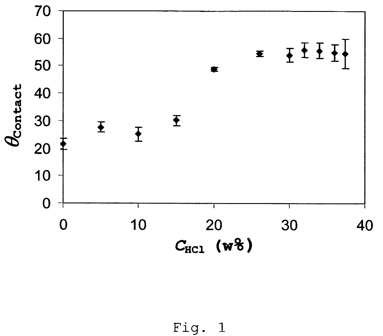
[0090]The spin coating technique was used to prepare standard wafers.

[0091]Multi-element solutions were prepared by dilution of ICP-MS calibration standards (1000 mg / L, nitrate s...


PUM

PropertyMeasurementUnit
contact angleaaaaaaaaaa

Abstract

The present invention provides an impurity measuring method comprising the steps of dropping a drop of a first solution on the surface of a substrate to be measured, moving the drop dropped on the surface of the substrate so that the drop is kept in contact with the surface and collects an impurity absorbed on the surface, recovering the drop after the movement and analyzing the recovered drop by chemical analysis to determine the type and concentration of the impurity, characterized in that the first solution is phobic to the substrate and the substrate consists substantially of Ge. The method is of particular importance for measuring metallic contamination on the surface of Ge substrates.

Description

RELATED APPLICATION[0001]This application claims the benefit of U.S. Provisional Application No. 60 / 530,214, filed Dec. 12, 2003, the contents of which are hereby incorporated by reference in their entirety and are hereby made a part of this specification.FIELD OF THE INVENTION[0002]The present invention relates to a method for impurity measurements on Ge substrates.BACKGROUND OF THE INVENTION[0003]In microelectronics industry Ge wafers are important substrates with technological applications in optical devices and are very recently introduced as a replacement for Si substrates for advanced Integrated Circuit (IC) devices. In order to realize high performance devices the Ge wafer surface has to be of high purity.[0004]Earlier studies have demonstrated the detrimental effects of metallic contaminants on the electro-physical properties of the Ge surface. Therefore, it is needed to control carefully the metallic contamination during processing of Ge wafers. Specifications for metallic ...

Claims


Application Information

Patent Timeline
Patent Type & Authority Patents(United States)
IPC IPC(8): G01N1/00G01N1/02G01N1/18G01N1/38G01N31/00G01R31/26H01L21/66
CPCG01N1/02Y10T436/255G01N2001/383G01N2001/028
Inventor HELLIN, DAVIDTEERLINCK, IVOSTEENBERGEN, JAN VAN
Owner N V UMICORE
Why Eureka
Try Eureka