Organic semiconductor material, organic semiconductor structure and organic semiconductor apparatus

a technology of organic semiconductors and organic semiconductors, applied in the direction of organic chemistry, solid-state devices, thermoelectric devices, etc., can solve the problems of reduced on/off ratio and disadvantageous likely to undergo oxidation, and achieve reduced ionization potential, prevent a rise in off current, and large on/off ratio

Inactive Publication Date: 2008-08-05
DAI NIPPON PRINTING CO LTD
View PDF6 Cites 0 Cited by
  • Summary
  • Abstract
  • Description
  • Claims
  • Application Information

AI Technical Summary

Benefits of technology

[0011]In the organic semiconductor material having the above structure according to the present invention, since A1, A2, B1, B2 and X in chemical formula 1 have the above π electron ring-containing skeleton structure, the planarity of A1-X-A2 as the main chain is disintegrated due to the steric hindrance, based on the presence of the aromatic ring located on the side chain part, between B1 and X and between B2 and X. The organic semiconductor material having this structure is advantageously less likely to undergo oxidation even under the atmospheric environment at the time of film formation, has excellent stability in the course of production and, at the same time, can form an organic semiconductor layer which can prevent a rise in off current to realize a large on / off ratio. The low susceptibility to oxidation of the organic semiconductor material according to the present invention is considered attributable to a lowering in ionization potential based on the loss of the planarity of the main chain part. Further, since B1 and B2 have an alkyl chain, the organic semiconductor material according to the present invention has at least a certain level of solubility in solvents and consequently can realize film formation by various coating or printing means, which is advantageous from the viewpoint of production. Further, the organic semiconductor material according to the present invention has T conjugated system extended structure and thus is advantageous for narrowing the band gap and, at the same time, can suppress a rise in ionization potential.
[0023]The organic semiconductor structure and organic semiconductor device according to the present invention comprises an organic semiconductor layer that can prevent a rise in off current to realize a large on / off ratio. Further, since the organic semiconductor materials are regularly aligned in a main chain oriented form, intramolecular conduction is likely to occur. Further, since a packing structure, in which superimposition of π conjugated system of polymer chains on top of each other is spread multidimensionally, is formed, in the organic semiconductor layer, charges are likely to cause hopping conduction between the polymer chains. This is advantageous from the viewpoint of improving the charge mobility. Further, since the organic semiconductor layer is flexible and, at the same time, is highly mechanically durable, the organic semiconductor structure and organic semiconductor device are particularly useful, for example, for large-area display devices, for example, large-area image sensors, electronic papers, and other display media, comprising an organic semiconductor structure or an organic semiconductor device provided on a flexible plastic substrate.

Problems solved by technology

The organic semiconductor layer formed of polythiophenes such as poly(3-hexylthiophene) represented by chemical formula a is disadvantageously likely to undergo oxidation by oxygen in the air exposed during film formation.
TFT comprising an oxidized organic semiconductor layer suffers from a problem that the on / off ratio is reduced due to a rise in off current.

Method used


Image

  • Organic semiconductor material, organic semiconductor structure and organic semiconductor apparatus
  • Organic semiconductor material, organic semiconductor structure and organic semiconductor apparatus
  • Organic semiconductor material, organic semiconductor structure and organic semiconductor apparatus

Examples


example 1

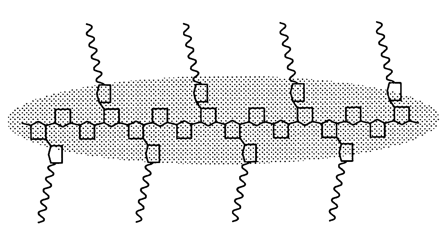
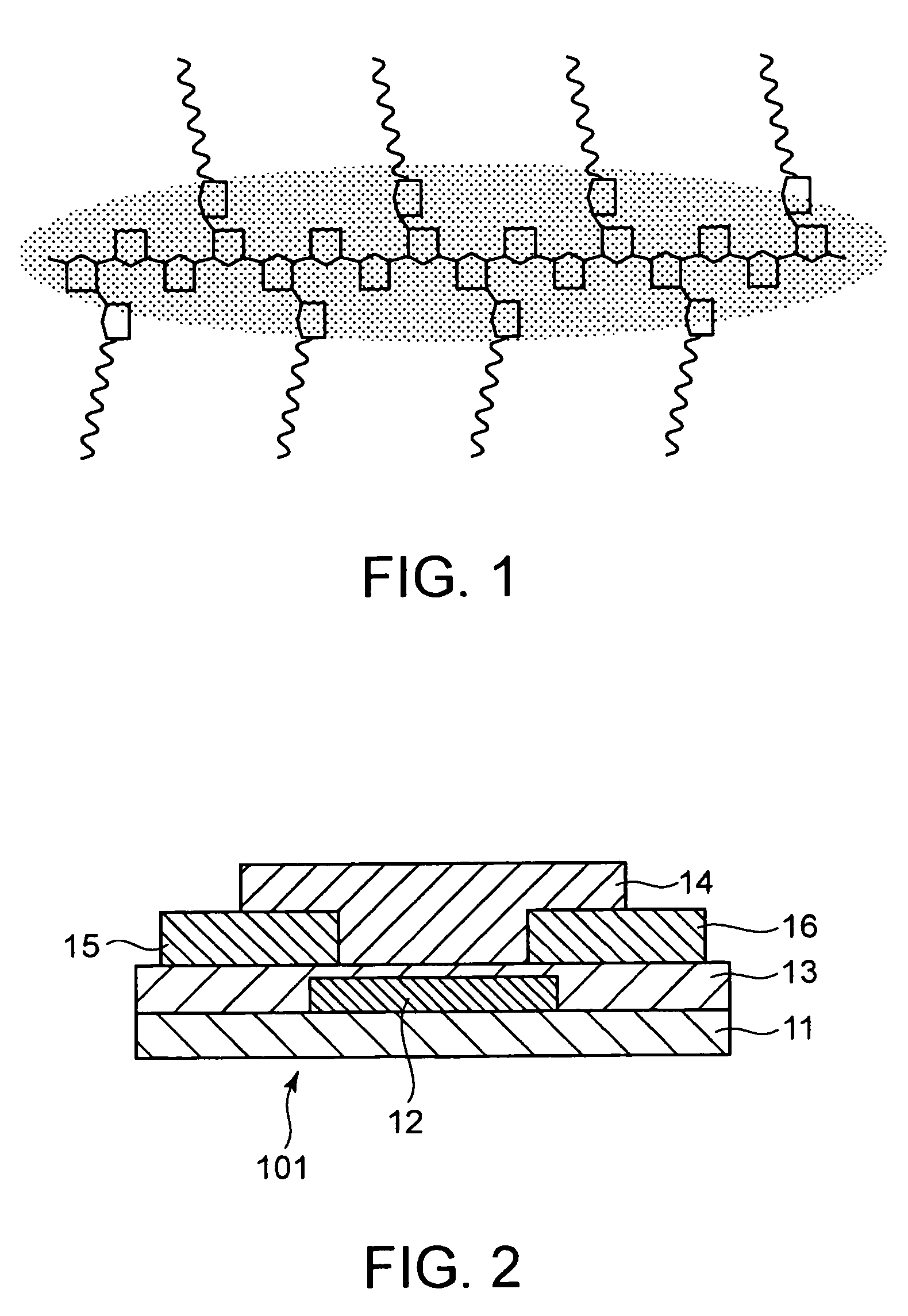
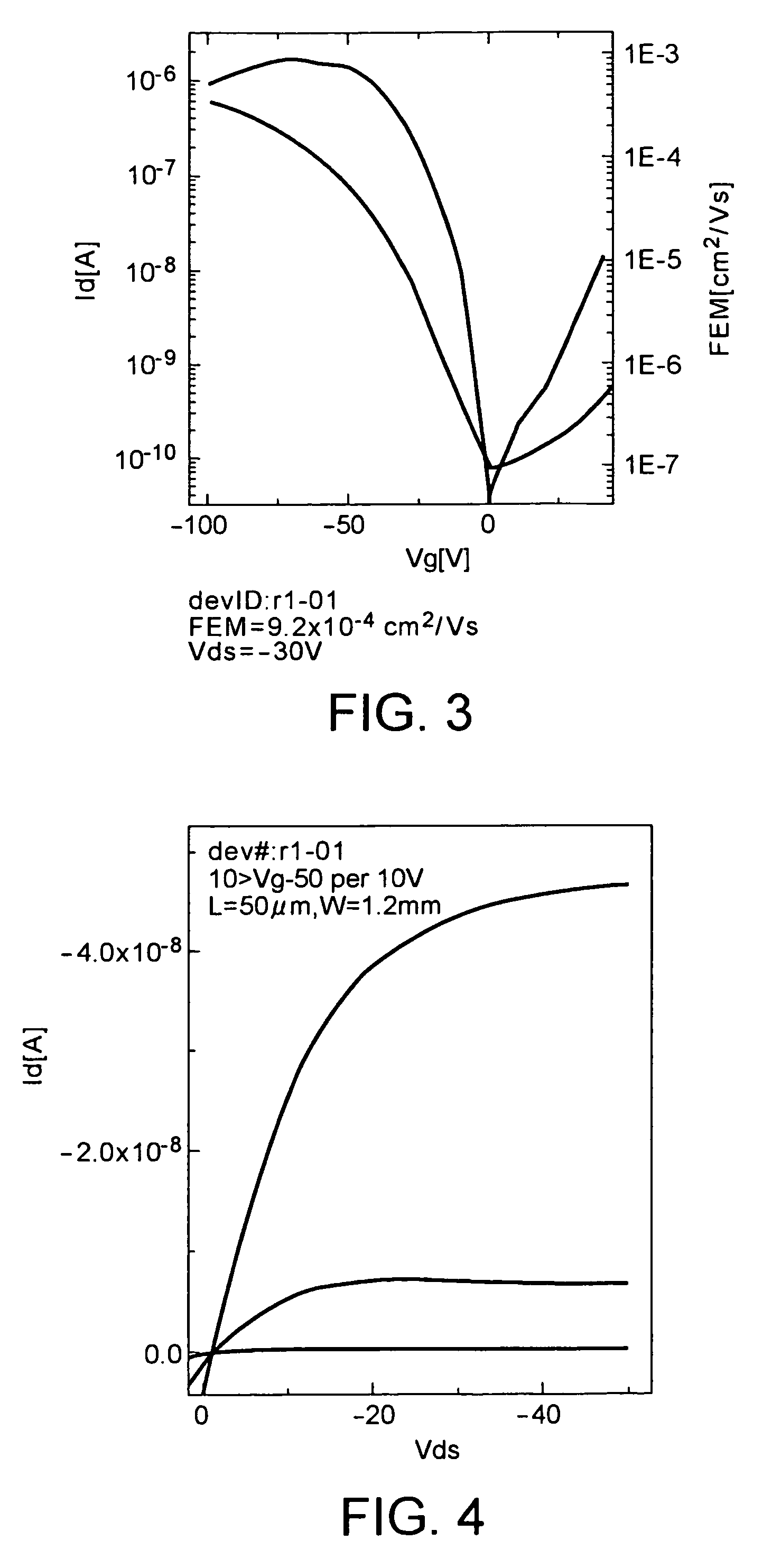
[0064]An organic semiconductor material represented by chemical formula 2, wherein R1 and R2 represent a C12 identical straight chain alkyl group, and having a number average molecular weight of about 55,000 and a weight average molecular weight of about 99,000, was prepared.

[0065]

[0066]

[0067]Thiophene (51.2 g, 623 mmol, 1.2 eq) was first placed in a three-necked flask equipped with a dropping funnel and a reflux tube. The atmosphere in the flask was replaced by Ar (argon), 200 ml of dehydrated tetrahydrofran (hereinafter referred to as “THF”) was then added thereto, and the mixture was stirred. The reaction solution was cooled to −78° C., 2.6 M n-BuLi (200 ml, 520 mmol, 1.0 eq) was added dropwise to the cooled solution, and the mixture was stirred for 30 min. The reaction solution was brought to 0° C. and was stirred for 2 hr. Thereafter, the reaction solution was brought to room temperature and was stirred for 15 min, followed by cooling to 0° C. 1-Bromo-n-dodecane (130 g, 520 mmo...

example 2

[0094]In Example 2, the effect of reducing ionization potential of the organic semiconductor material according to the present invention and the extension effect of the π conjugated system were studied. Stereoregular poly(3-hexylthiophene) which comprises thiophene as a main chain part and has high planarity (hereinafter referred to as “P3HT”) was used as a comparative material (see chemical formula a). This P3HT is known to have high semiconductor characteristics, but on the other hand, the stability in the air is so low that suitability for process is low, that is, the preparation of good transistor is difficult. A commercially available product of Merck was used as the P3HT.

[0095]

[0096]P3HT and the polymer material (name of compound: poly[3,3″′-bis(5-dodecyl-2-thienyl)-2,2′:5′,2″:5″,2′″-quaterthiophene], a compound represented by chemical formula 2 wherein R1 and R2 represent a straight chain alkyl group represented by —C12H25) according to the present invention were dissolved in...


PUM

PropertyMeasurementUnit
temperatureaaaaaaaaaa
thicknessaaaaaaaaaa
thicknessaaaaaaaaaa

Abstract

An organic semiconductor material characterized by having a structure represented by chemical formula 1, the planarity of a main chain A1-X-A2 being disintegrated by steric hindrance between B1 and X and steric hindrance between B2 and X, the organic semiconductor material having a number average molecular weight of about 2,000 to about 200,000:wherein A1, A2, B1, B2 and X each have a skeleton structure comprising L 6 π electron rings, M 8 π electron rings, N 10 π electron rings, O 12 π electron rings, P 14 π electron rings, Q 16 π electron rings, R 18 π electron rings, S 20 π electron rings, T 22 π electron rings, U 24 π electron rings, and V 26 π electron rings, wherein L, M, N, O, P, Q, R, S, T, U, and V are each an integer of 0 (zero) to 6 and L+M+N+O+P+Q+R+S+T+U+V=1 to 6; and B1 and B2 have an alkyl group.

Description

TECHNICAL FIELD[0001]The present invention relates to a liquid crystalline organic semiconductor material, which is highly stable under a film forming environment and, at the same time, can easily form a film, for example, by coating, an organic semiconductor structure and an organic semiconductor device.BACKGROUND ART[0002]Attention has recently been drawn to studies on organic semiconductor structures using an organic semiconductor material, and application of organic semiconductor structures to various devices has been expected. Devices utilizable, for example, in large-area flexible display devices, for example, thin-film transistors (also known as “organic TFTs”), luminescent elements, and solar cells are being studied for such application.[0003]In order to utilize organic semiconductor structures on a practical level, the organic semiconductor layer formed of an organic semiconductor material should exhibit stable charge mobility in a wide service temperature range, and, at th...

Claims


Application Information

Patent Timeline
Patent Type & Authority Patents(United States)
IPC IPC(8): H01L51/30C07D333/10
CPCC08G61/126C08G83/005H01L51/0036Y02E10/549H01L51/0545H10K85/113H10K10/466
Inventor SUGAWARA, SHIGERUMAEDA, HIROKITOMINO, KENMATSUOKA, MASANAO
Owner DAI NIPPON PRINTING CO LTD
Why Eureka
Try Eureka