Organic light emitting display device and method of fabricating the same

a technology of light-emitting display and organic light-emitting layer, which is applied in the direction of organic semiconductor devices, discharge tubes/lamp details, discharge tubes luminescnet screens, etc., can solve the problems of large gap between the donor substrate and the pixel electrode, damage and deterioration of the organic emission layer, and difficulty in fabricating a large-sized devi

Active Publication Date: 2008-08-05
SAMSUNG DISPLAY CO LTD
View PDF7 Cites 25 Cited by
  • Summary
  • Abstract
  • Description
  • Claims
  • Application Information

AI Technical Summary

Benefits of technology

[0009]It is therefore an object of the present invention to provide an improved design for an organic light emitting display device and an improved method of making the same.
[0010]It is further an object of the present invention to provide an improved design and method of making that reduces the gap in the LITI process.
[0011]These and other objects can be achieved by an organic light emitting display device and a method of fabricating the same, in which a dummy pattern is provided under a pixel electrode of an emission region, so that a distance between a donor substrate and the pixel electrode is minimized, thus enhancing the efficiency of laser energy in a LITI process, and improving the life span and efficiency of an organic layer.

Problems solved by technology

Further, a metal mask is needed to pattern the emission layer by the deposition process, so that there is much trouble in fabricating a large-sized device.
However, in typical LITI processes for forming an organic light emitting display device, a large gap exists between the donor substrate and the pixel electrode.
This large gap requires more laser energy for the LITI process, leading to damage and deterioration of the organic emission layer.

Method used


Image

  • Organic light emitting display device and method of fabricating the same
  • Organic light emitting display device and method of fabricating the same
  • Organic light emitting display device and method of fabricating the same

Examples


Embodiment Construction

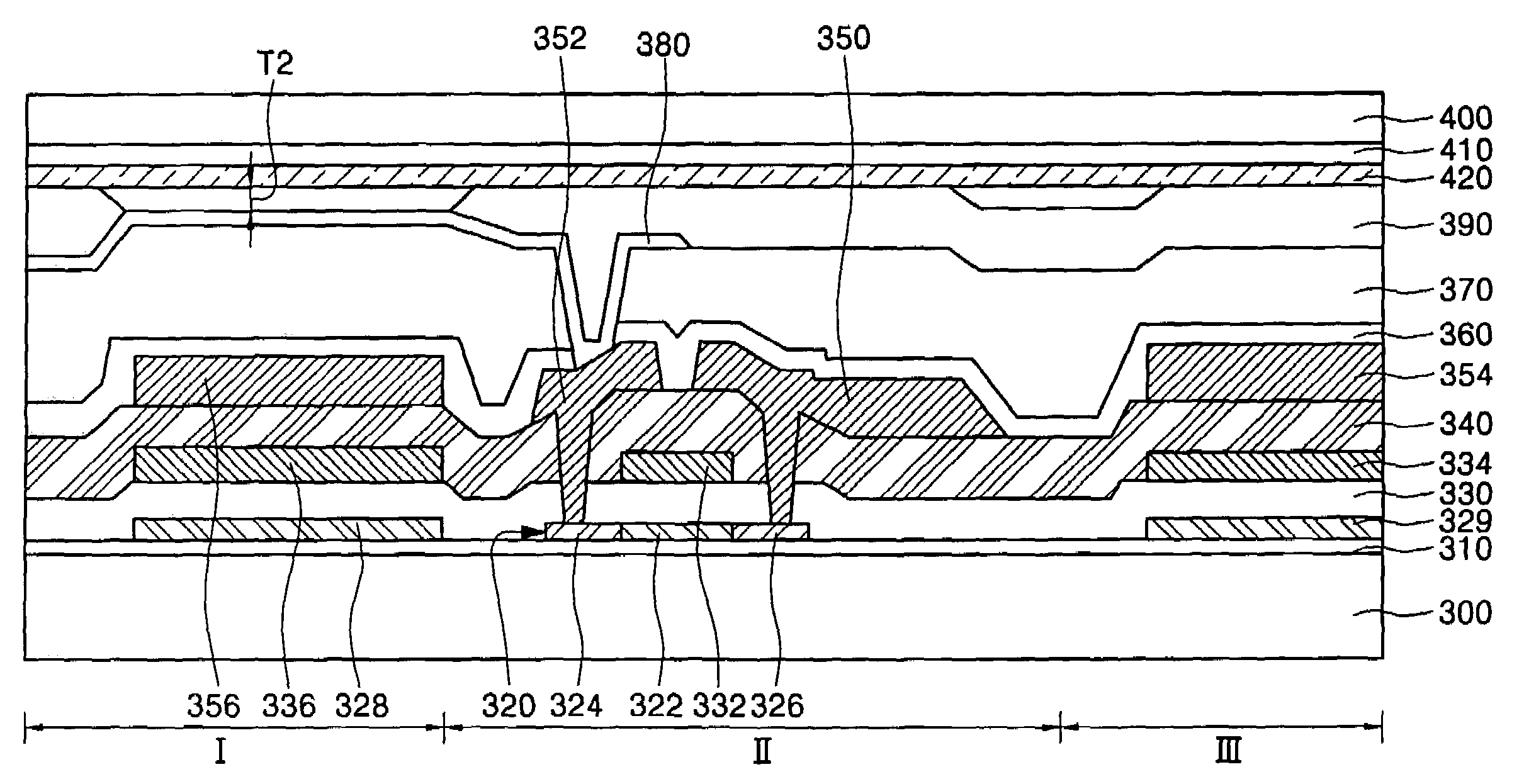
[0018]A method of fabricating an organic light emitting display device will be described in conjunction with FIG. 1. FIG. 1 is a cross-sectional view of an organic light emitting display device, which includes an emission region I, a thin film transistor region II, and a capacitor region III.

[0019]To begin, a buffer layer 110 is formed on a substrate 100. Preferably, the buffer layer 110 is used to prevent impurities in the substrate 100 from migrating into the device formed in a subsequent process. Subsequently, an amorphous silicon layer (not shown) is formed as a semiconductor layer having a predetermined thickness on the buffer layer 110. Then, the amorphous silicon layer is crystallized by excimer laser annealing (ELA), sequential lateral solidification (SLS), metal induced crystallization (MIC), metal induced lateral crystallization (MILC), or the like. The crystallized silicon layer is patterned by a photolithography process, thus forming a polysilicon layer pattern 120 in th...


PUM


Abstract

An organic light emitting display device and a method of fabricating the same. A dummy pattern is formed in an emission region to increase the step height of the emission region by an electrode material while a thin film transistor is fabricated, so that a distance between a pixel electrode and a donor film is decreased during fabrication of an organic layer. This reduced distance reduces laser energy for transfer using laser-induced thermal imaging, thus improving life span and efficiency of the device. Further, the pixel electrode can extend into a thin film transistor region and a capacitor region, thus enhancing an aperture ratio.

Description

CLAIM OF PRIORITY[0001]This application makes reference to, incorporates the same herein, and claims all benefits accruing under 35 U.S.C. §119 from an application earlier filed in the Korean Intellectual Property Office on 13 Dec. 2004 and there duly assigned Serial No. 10-2004-0105146.BACKGROUND OF THE INVENTION[0002]1. Field of the Invention[0003]The present invention relates to an organic light emitting display device and a method of fabricating the same, and more particularly, to an organic light emitting display device with a pixel region having an increased step difference to facilitate the deposition of an organic layer using a laser-induced thermal imaging method.[0004]2. Description of the Related Art[0005]Among flat panel display devices, an organic light emitting display device has a fast response time shorter than 1 ms, consumes little power, and has a wide viewing angle range because it can emit light by itself. As a result, the organic light emitting display device ha...

Claims


Application Information

Patent Timeline
Patent Type & Authority Patents(United States)
IPC IPC(8): H01L29/04H01L29/10H01L31/00
CPCH01L27/3223H01L51/0013H01L27/3244H01L27/1214H01L27/13H01L2251/5315H01L51/56H01L27/1255H10K59/88H10K71/18H10K59/12H10K2102/3026H10K71/00H05B33/26H05B33/10
Inventor KANG, TAE-WOOK
Owner SAMSUNG DISPLAY CO LTD
Why Eureka
Try Eureka