Method and apparatus for measuring device mismatches

a technology of mismatching and measuring devices, applied in the direction of digital storage, instrumentation, marginal circuit testing, etc., can solve the problems of large number of cells, difficult computer-aided physical design, and large number of connections between cells, and achieve the effect of high spatial resolution of measurements

Active Publication Date: 2008-08-05
GLOBALFOUNDRIES US INC
View PDF3 Cites 16 Cited by
  • Summary
  • Abstract
  • Description
  • Claims
  • Application Information

AI Technical Summary

Benefits of technology

[0012]It is therefore one object of the present invention to provide an improved method of testing an array of electronic devices which provides high spatial resolution of measurements, e.g., capable of measuring current mismatches between two minimal strength devices in close proximity.
[0013]It is another object of the present invention to provide such a method which may be implemented in an array having a large number of devices under test while reducing or minimizing resource cost.

Problems solved by technology

An IC may include a very large number of cells and require complicated connections between the cells.
Due to the large number of components and the details required by the fabrication process for very large scale integrated (VLSI) devices, physical design is not practical without the aid of computers.
While the outputs of circuit 10 provide a fair basis to characterize the response of the devices, the measurements are not completely accurate since they fail to take into consideration various effects on signal creation and transmission.
Calibration of the measurement circuitry does not compensate for variations in the loading effects.
Moreover, spatial variability in integrated circuits is becoming worse due to variations such as Leff variation, doping concentrations, spurious leakage, systematic variation due to chemical mechanical planarization, etc.
Existing test structures cannot adequately account for the variability in these measurements.
In order to reliably characterize the variabilities, hundreds of samples are needed, which is even more impractical given the limited number of input / output (C4) pads provided on the circuits.
Circuit designers make assumptions about spatial variations of parameters which have a significant impact on product performance, but there is no reliable system for verifying these assumptions.

Method used


Image

  • Method and apparatus for measuring device mismatches
  • Method and apparatus for measuring device mismatches
  • Method and apparatus for measuring device mismatches

Examples


Embodiment Construction

)

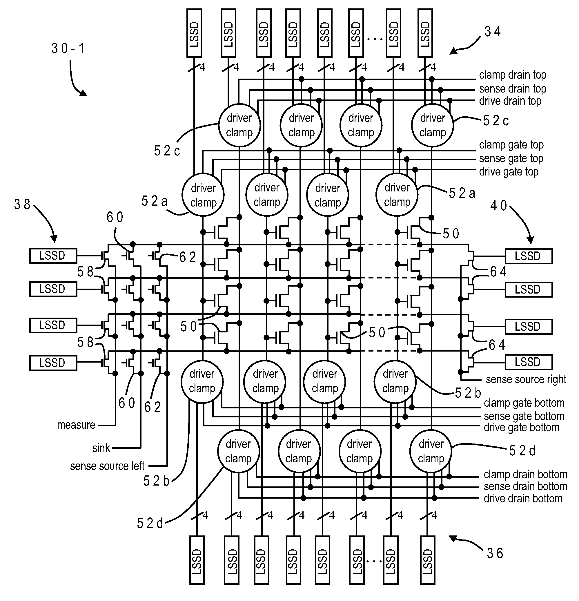
[0025]The present invention is directed to an improved method and apparatus for measuring mismatches in electronic devices. Local device mismatches have short correlation distances, so characterization of random mismatches requires test structures with closely placed devices wherein each device can effectively be measured individually. The structures disclosed herein are useful for such statistical characterization of intrinsic parameter fluctuations in metal-oxide semiconducting field-effect transistor (MOSFET) devices. The test structures feature a large array of densely populated SRAM-sized devices that allow fast and precise measurement of electrical characteristics of each individual device. These structures may be used to characterize the variations in device parameters for different threshold implantation levels in a 65 nm silicon-on-insulator (SOI) process.

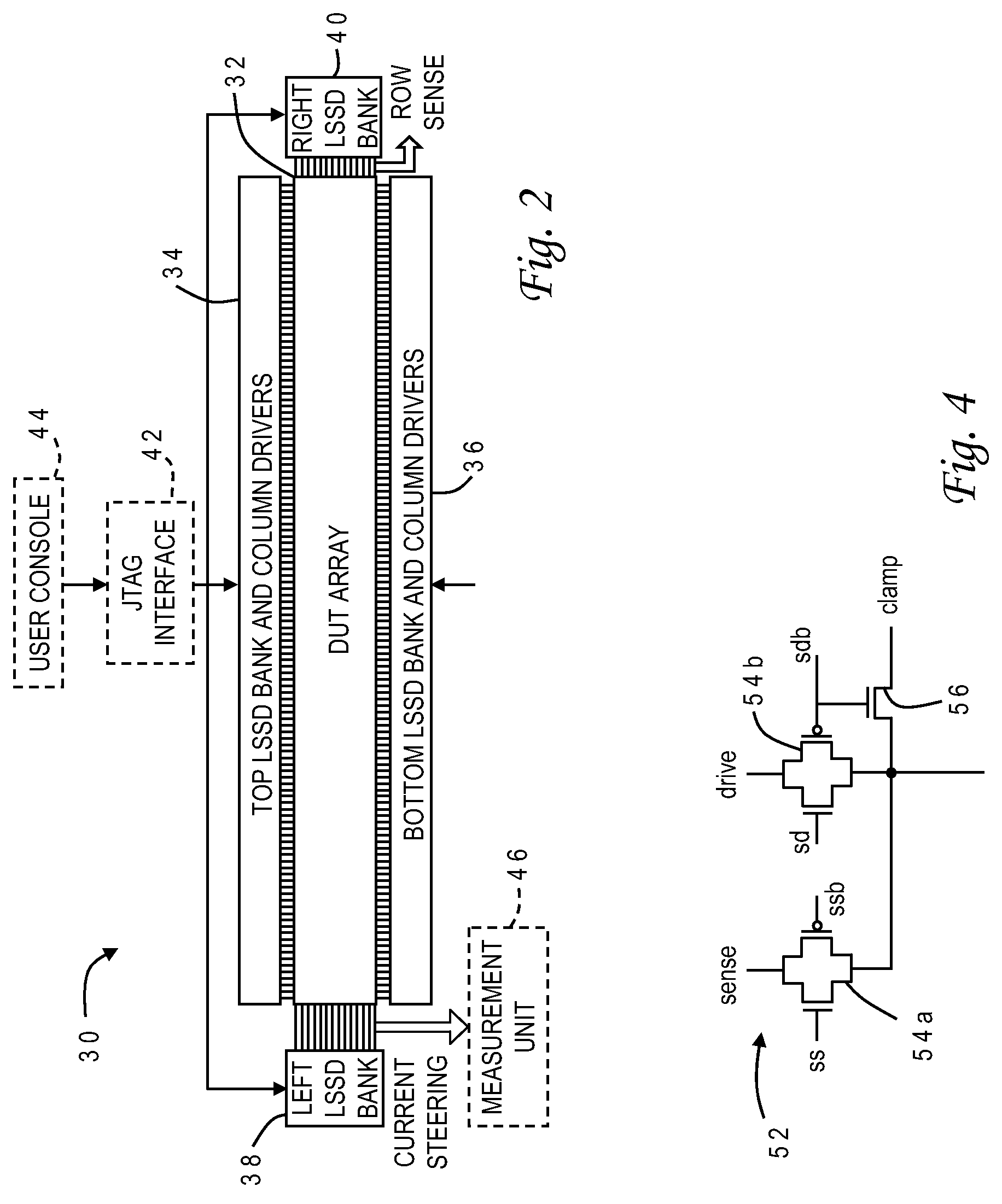
[0026]With reference now to the figures, and in particular with reference to FIG. 2, there is depicted a layout for one...


PUM


Abstract

A test structure for statistical characterization of local device mismatches contains densely populated SRAM devices arranged in a row / column addressable array that enables resource sharing of many devices. The test structure includes a built-in sensing mechanism to calibrate or null out sources of error, and current steering to avoid negative effects of current leakage along spurious paths. The gate and drain lines of each column are driven from both the top and bottom to minimizes parasitic effects. The system can handle a large number of devices while still providing high spatial resolution of current measurements.

Description

BACKGROUND OF THE INVENTION[0001]1. Field of the Invention[0002]The present invention generally relates to the design and testing of integrated circuits, and more particularly to a method and system for testing an array of electronic devices formed on an integrated circuit.[0003]2. Description of the Related Art[0004]Integrated circuits are used for a wide variety of electronic applications, from simple devices such as wristwatches, to the most complex computer systems. A microelectronic integrated circuit (IC) chip can generally be thought of as a collection of logic cells with electrical interconnections between the cells, formed on a semiconductor substrate (e.g., silicon). An IC may include a very large number of cells and require complicated connections between the cells. A cell is a group of one or more circuit elements such as transistors, capacitors, resistors, inductors, and other basic circuit elements grouped to perform a logic function. Cell types include, for example, c...

Claims


Application Information

Patent Timeline
Patent Type & Authority Patents(United States)
IPC IPC(8): G01R31/26
CPCG01R31/3004G11C29/02G11C29/12005G11C29/50G11C11/41G11C2029/5006G11C2029/1202G11C2029/1204G11C2029/5004
Inventor AGARWAL, KANAK B.LIU, YINGMCDOWELL, CHANDLER T.NASSIF, SANI R.PLUSQUELLIC, JAMES F.SIVAGNANAME, JAYAKUMARAN
Owner GLOBALFOUNDRIES US INC
Why Eureka
Try Eureka